FCT162511AT(2001) 查看數據表(PDF) - Integrated Device Technology
零件编号
产品描述 (功能)
比赛名单
FCT162511AT
(Rev.:2001)
(Rev.:2001)
Integrated Device Technology

FCT162511AT Datasheet PDF : 10 Pages
| |||
IDT54/74FCT162511AT/CT
FAST CMOS 16-BIT REGISTERED/LATCHED TRANSCEIVER
MILITARY AND INDUSTRIAL TEMPERATURE RANGES
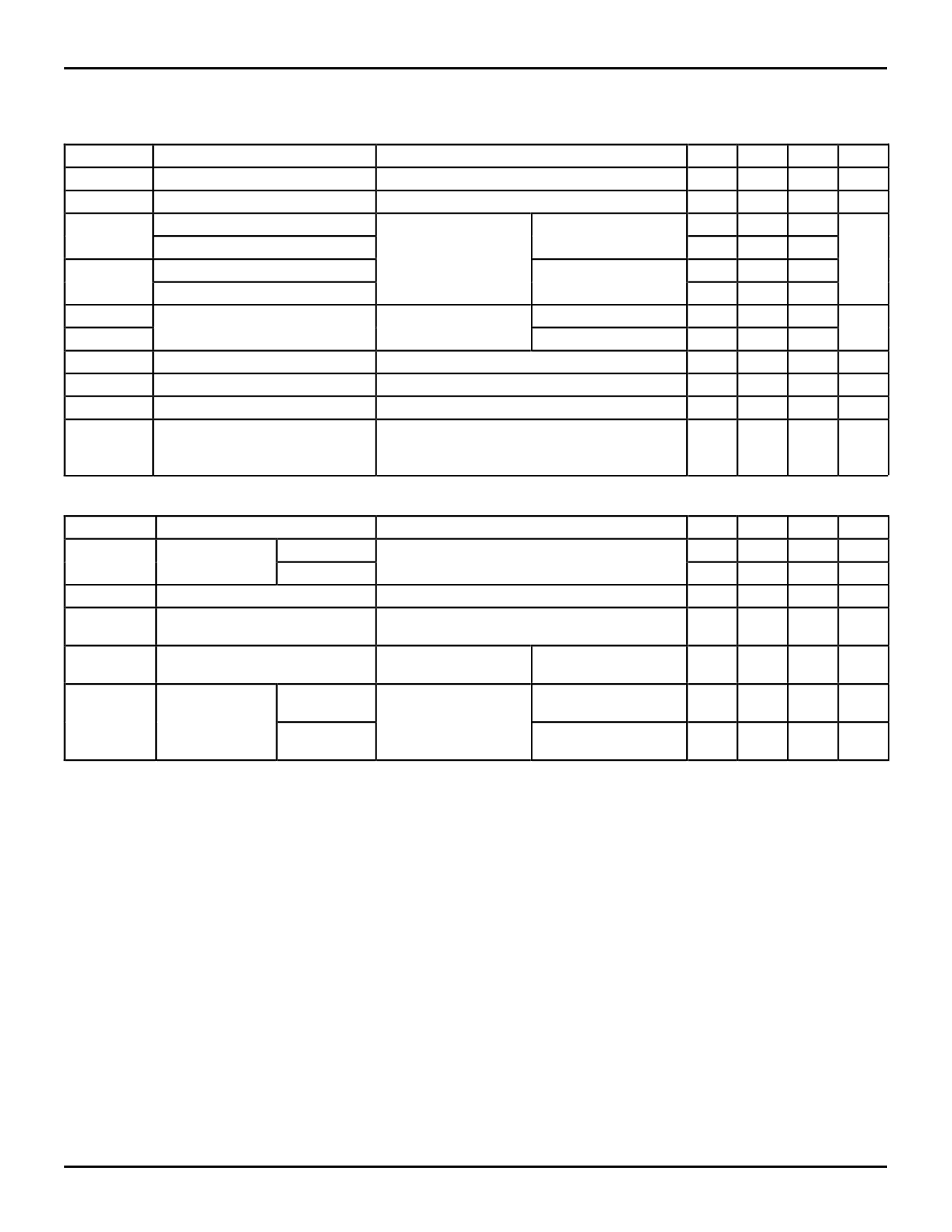
POWER SUPPLY CHARACTERISTICS
Symbol
Parameter
Test Conditions(1)
∆ICC
Quiescent Power Supply Current VCC = Max.
TTL Inputs HIGH
VIN = 3.4V(3)
All other Input Pins
Parity Input Pins (PAx, PBx)
ICCD
Dynamic Power Supply
Current(4)
VCC = Max.
Outputs Open
OEAB = GND, OEBA = VCC
One Input Togging
50% Duty Cycle
VIN = VCC
VIN = GND
IC
Total Power Supply Current(6)
VCC = Max.
Outputs Open
fCP = 10MHz (CLKAB)
50% Duty Cycle
OEAB = GND, OEBA = VCC
VIN = VCC
VIN = GND
LEAB = GND
One Bit Toggling
fi = 5MHz
50% Duty Cycle
VIN = 3.4V
VIN = GND
VCC = Max.
Outputs Open
fCP = 10MHz (CLKAB)
50% Duty Cycle
OEAB = GND, OEBA = VCC
VIN = VCC
VIN = GND
LEAB = GND
Eighteen Bits Toggling
fi = 2.5MHz
50% Duty Cycle
VIN = 3.4V
VIN = GND
Min. Typ.(2) Max.
Unit
—
0.5
1.5
mA
—
1
2.5
—
75
120
µA/
MHz
—
0.8
1.7
mA
—
1.3
3.2
—
3.8
6.5(5)
—
9
21.8(5)
NOTES:
1. For conditions shown as Min. or Max., use appropriate value specified under Electrical Characteristics for the applicable device type.
2. Typical values are at VCC = 5.0V, +25°C ambient.
3. Per TTL driven input (VIN = 3.4V). All other inputs at VCC or GND.
4. This parameter is not directly testable, but is derived for use in Total Power Supply Calculations.
5. Values for these conditions are examples of the ICC formula. These limits are guaranteed but not tested.
6. IC = IQUIESCENT + IINPUTS + IDYNAMIC
IC = ICC + ∆ICC DHNT + ICCD (fCPNCP/2 + fiNi)
ICC = Quiescent Current (ICCL, ICCH and ICCZ)
∆ICC = Power Supply Current for a TTL High Input (VIN = 3.4V)
DH = Duty Cycle for TTL Inputs High
NT = Number of TTL Inputs at DH
ICCD = Dynamic Current caused by an Input Transition Pair (HLH or LHL)
fCP = Clock Frequency for Register Devices (Zero for Non-Register Devices)
NCP = Number of Clock Inputs at fCP
fi = Input Frequency
Ni = Number of Inputs at fi
6
Share Link: