FCT162511AT 查看數據表(PDF) - Integrated Device Technology
零件编号
产品描述 (功能)
比赛名单
FCT162511AT Datasheet PDF : 11 Pages
| |||
IDT54/74FCT162511AT/CT
FAST CMOS 16-BIT REGISTERED/LATCHED TRANSCEIVER WITH PARITY
MILITARY AND COMMERCIAL TEMPERATURE RANGES
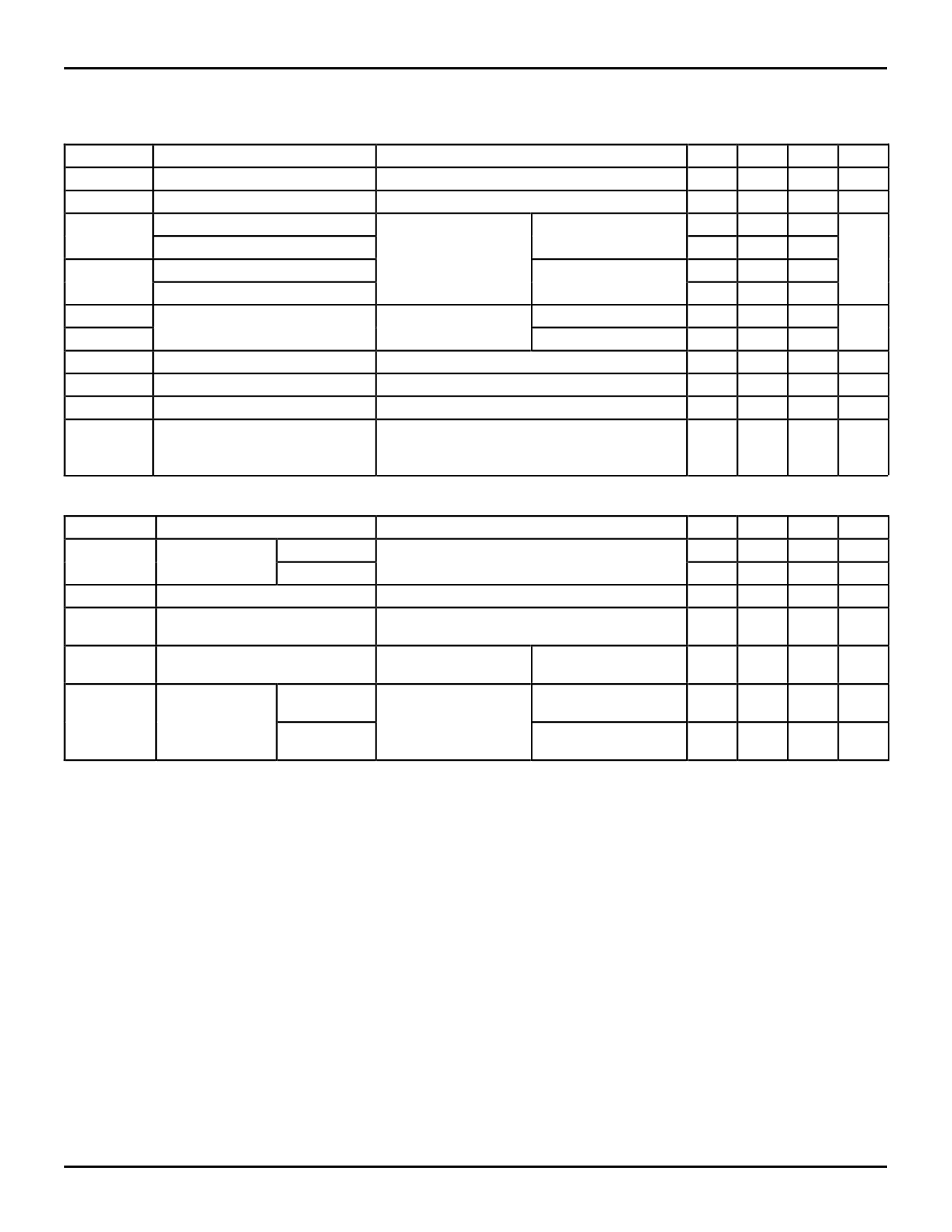
DC ELECTRICAL CHARACTERISTICS OVER OPERATING RANGE
Following Conditions Apply Unless Otherwise Specified:
Commercial: TA = –40°C to +85°C, VCC = 5.0V ± 10%; Military: TA = –55°C to +125°C, VCC = 5.0V ± 10%
Symbol
VIH
Parameter
Input HIGH Level
Test Conditions(1)
Guaranteed Logic HIGH Level
Min. Typ.(2) Max. Unit
2.0 —
—
V
VIL
Input LOW Level
Guaranteed Logic LOW Level
II H
Input HIGH Current (Input pins)(5) VCC = Max.
VI = VCC
Input HIGH Current (I/O pins)(5)
II L
Input LOW Current (Input pins)(5)
VI = GND
Input LOW Current (I/O pins)(5)
—
— 0.8
V
—
—
±1 µA
—
—
±1
—
—
±1
—
—
±1
IOZH
IOZL
High Impedance Output Current
(3-State Output pins)(5)
VCC = Max.
VO = 2.7V
VO = 0.5V
—
—
±1 µA
—
—
±1
VIK
Clamp Diode Voltage
IOS
Short Circuit Current
VCC = Min., IIN = –18mA
VCC = Max., VO = GND(3)
— –0.7 –1.2 V
–80 –140 –225 mA
VH
Input Hysteresis
—
— 100 — mV
ICCL
ICCH
ICCZ
Quiescent Power Supply Current VCC = Max., VIN = GND or VCC
OUTPUT DRIVE CHARACTERISTICS FOR FCT162511T
—
5
500 µA
2916 lnk 07
Symbol
IODL
Parameter
Output LOW
(I/O pins)
Test Conditions(1)
VCC = 5V, VIN = VIH or VIL, VOUT = 1.5V(3)
Min. Typ.(2) Max.
60 115 200
Unit
mA
IODH
Current
(Open Drain)
Output HIGH Current (I/O pins)
VCC = 5V, VIN = VIH or VIL, VOUT = 1.5V(3)
— 250 —
mA
–60 –115 –200 mA
IOFF
Output Power Off Leakage
Current (Open Drain)(5)
VCC = 0, VO ≤ 5.5V
—
—
±1
VOH
Output HIGH Voltage (I/O pins) VCC = Min.
VIN = VIH or VIL
IOH = –16mA MIL.
2.4 3.3 —
IOH = –24mA COM'L.
VOL
Output LOW
(I/O pins)
VCC = Min.
Voltage
VIN = VIH or VIL
IOL = 16mA MIL.
IOL = 24mA COM'L.
— 0.3 0.55
(Open Drain)
IOL = 48mA MIL.
IOL = 64mA COM'L.
— 0.3 0.55
NOTES:
1. For conditions shown as Max. or Min., use appropriate value specified under Electrical Characteristics for the applicable device type.
2. Typical values are at Vcc = 5.0V, +25°C ambient.
3. Not more than one output should be tested at one time. Duration of the test should not exceed one second.
4. Duration of the condition can not exceed one second.
5. The test limit for this parameter is ± 5µA at TA = –55°C.
µA
V
V
V
2916 tbl 08
5.11
6
Share Link: 