IDT54FCT162501ATE 查看數據表(PDF) - Integrated Device Technology
零件编号
产品描述 (功能)
比赛名单
IDT54FCT162501ATE Datasheet PDF : 9 Pages
| |||
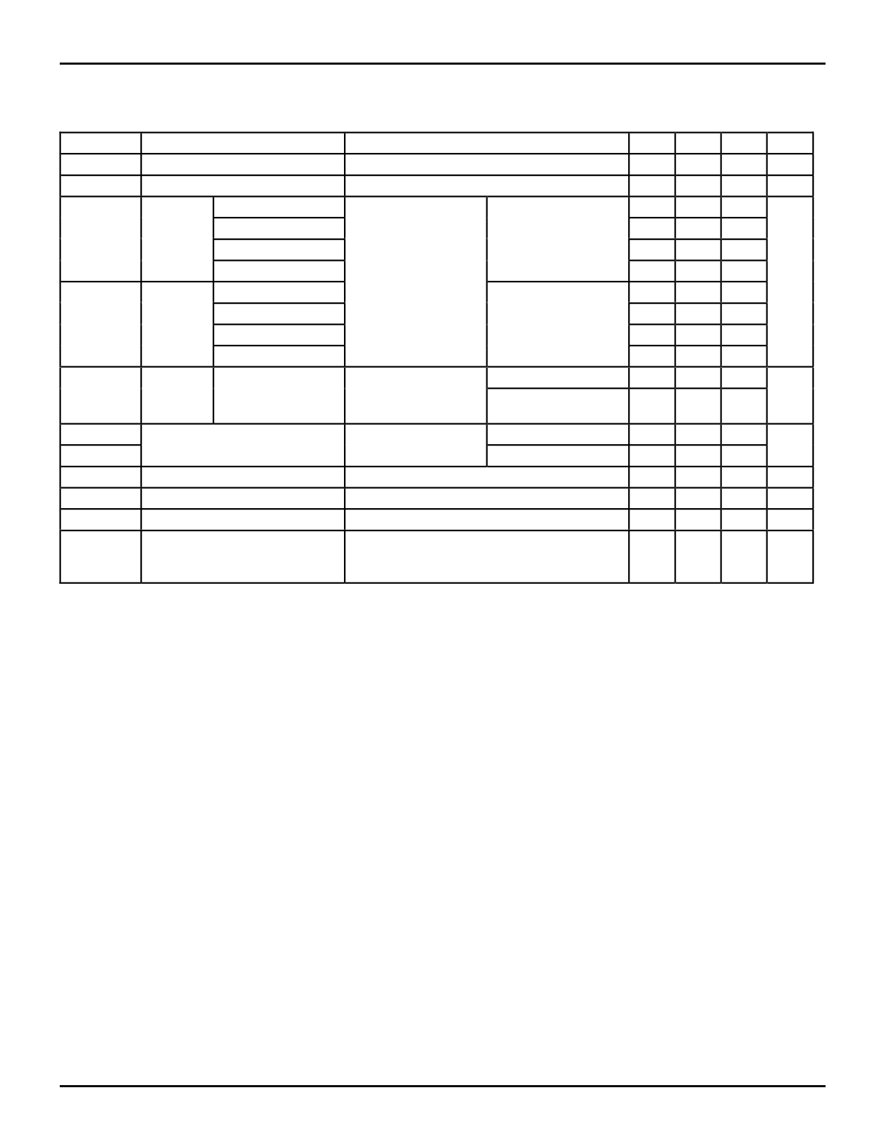
IDT54/74FCT16501AT/CT/ET, 162501AT/CT/ET, 162H501AT/CT/ET
FAST CMOS 18-BIT REGISTERED TRANSCEIVER
MILITARY AND COMMERCIAL TEMPERATURE RANGES
DC ELECTRICAL CHARACTERISTICS OVER OPERATING RANGE (BUS HOLD)
Following Conditions Apply Unless Otherwise Specified:
Commercial: TA = –40°C to +85°C, VCC = 5.0V ± 10%; Military: TA = –55°C to +125°C, VCC = 5.0V ± 10%
Symbol
VIH
Parameter
Input HIGH Level
Test Conditions(1)
Guaranteed Logic HIGH Level
Min. Typ.(2) Max.
2.0 —
—
VIL
Input LOW Level
Guaranteed Logic LOW Level
II H
Input
Standard Input(5)
VCC = Max.
VI = VCC
HIGH
Standard I/O(5)
Current(4) Bus-Hold Input
—
— 0.8
—
—
±1
—
—
±1
—
— ±100
Bus-Hold I/O
II L
Input
Standard Input(5)
LOW
Standard I/O(5)
Current(4) Bus-Hold Input
VI = GND
—
— ±100
—
—
±1
—
—
±1
—
— ±100
Bus-Hold I/O
—
— ±100
IBHH
Bus Hold Bus-Hold Input
VCC = Min.
VI = 2.0V
–50 —
—
IBHL
IOZH
IOZL
Sustain
Current(4)
High Impedance Output Current
(3-State Output pins)(5,6)
VCC = Max.
VI = 0.8V
VO = 2.7V
VO = 0.5V
+50 —
—
—
—
±1
—
—
±1
VIK
Clamp Diode Voltage
IOS
Short Circuit Current
VCC = Min., IIN = –18mA
VCC = Max., VO = GND(3)
— –0.7 –1.2
–80 –140 –225
VH
Input Hysteresis
—
— 100 —
ICCL
ICCH
ICCZ
Quiescent Power Supply Current VCC = Max., VIN = GND or VCC
—
5 500
NOTES:
1. For conditions shown as Max. or Min., use appropriate value specified under Electrical Characteristics for the applicable device type.
2. Typical values are at Vcc = 5.0V, +25°C ambient.
3. Not more than one output should be tested at one time. Duration of the test should not exceed one second.
4. Pins with Bus Hold are identified in the pin description.
5. The test limit for this parameter is ± 5µA at TA = –55°C.
6. Does not include Bus Hold I/O pins.
Unit
V
V
µA
µA
µA
V
mA
mV
µA
2547 lnk 08
5.10
5
Share Link: 