MX10C8051 查看數據表(PDF) - Unspecified
零件编号
产品描述 (功能)
比赛名单
MX10C8051 Datasheet PDF : 14 Pages
| |||
VCC
VCC
P0
ICC
VCC
EA
RST
MX10C805X
(NC)
XTAL2
XTAL1
VSS
All other pins disconnected
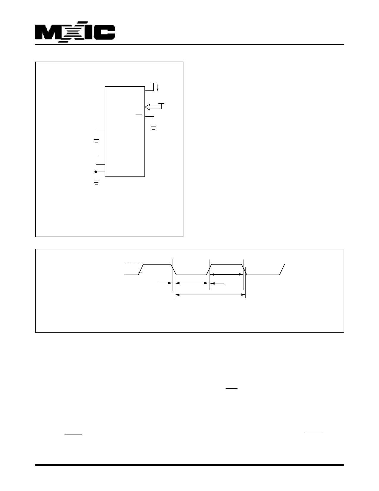
Figure 8. ICC Test Condition, Power Down Mode
VCC=2.0V to 6.0V
MX10C805X
VCC-0.5
0.45V
0.7 VCC
0.2 VCC-0.1
TCHCL
TCLCX
TCHCX
TCLCH
TCLCL
Figure 9. Clock Signal Waveform for ICC Tests in Active and Idle Modes.
TCLCH = TCHCL = 5 ns
EXPLANATION OF THE AC SYMBOLS
Each timing symbol has 5 characters. The first charac-
ter is always a "T" (stands for time). The other charac-
ters, depending on their positions, stand for the name of
a signal or the logical status of that signal. The following
is a list of all the characters and what they stand for.
A: Address
C: Clock
D: Input Data
H: Logic level HIGH
L: Logic level LOW, or ALE
P: PSEN
Q: Output Data
R: RD signal
T: Time
V: Valid
W: WR signal
X: No longer a valid logic level
Z: Float
For example,
TAVLL = Time from Address Valid to ALE Low
TLLPL = Time from ALE Low to PSEN Low
P/N:PM0591
REV. 0.3, APR. 09, 1999
8
Share Link: 