PI5L100 查看數據表(PDF) - Pericom Semiconductor Corporation
零件编号
产品描述 (功能)
比赛名单
PI5L100 Datasheet PDF : 13 Pages
| |||
PI5L100
12345678901234567890123456789012123456789012345678901234567890121234567890123456789012345L678a9n01S21w23i4t5c6h789Q01U23A456D78920:11234M567U89X01/2D12E34M567U89X012
Maximum Ratings
(Above which the useful life may be impaired. For user guidelines, not tested.)
Storage Temperature ................................................................. –65°C to +150°C
Ambient Temperature with Power Applied ..................................... 0°C to +70°C
Supply Voltage to Ground Potential (Inputs & Vcc Only) .......... –0.5V to +7.0V
Supply Voltage to Ground Potential (Outputs & D/O Only) ....... –0.5V to +7.0V
DC Input Voltage ......................................................................... –0.5V to +7.0V
DC Output Current ................................................................................... 120 mA
Power Dissipation ......................................................................................... 0.5W
Note:
Stresses greater than those listed under
MAXIMUM RATINGS may cause permanent
damage to the device. This is a stress rating
only and functional operation of the device at
these or any other conditions above those
indicated in the operational sections of this
specification is not implied. Exposure to
absolute maximum rating conditions for
extended periods may affect reliability.
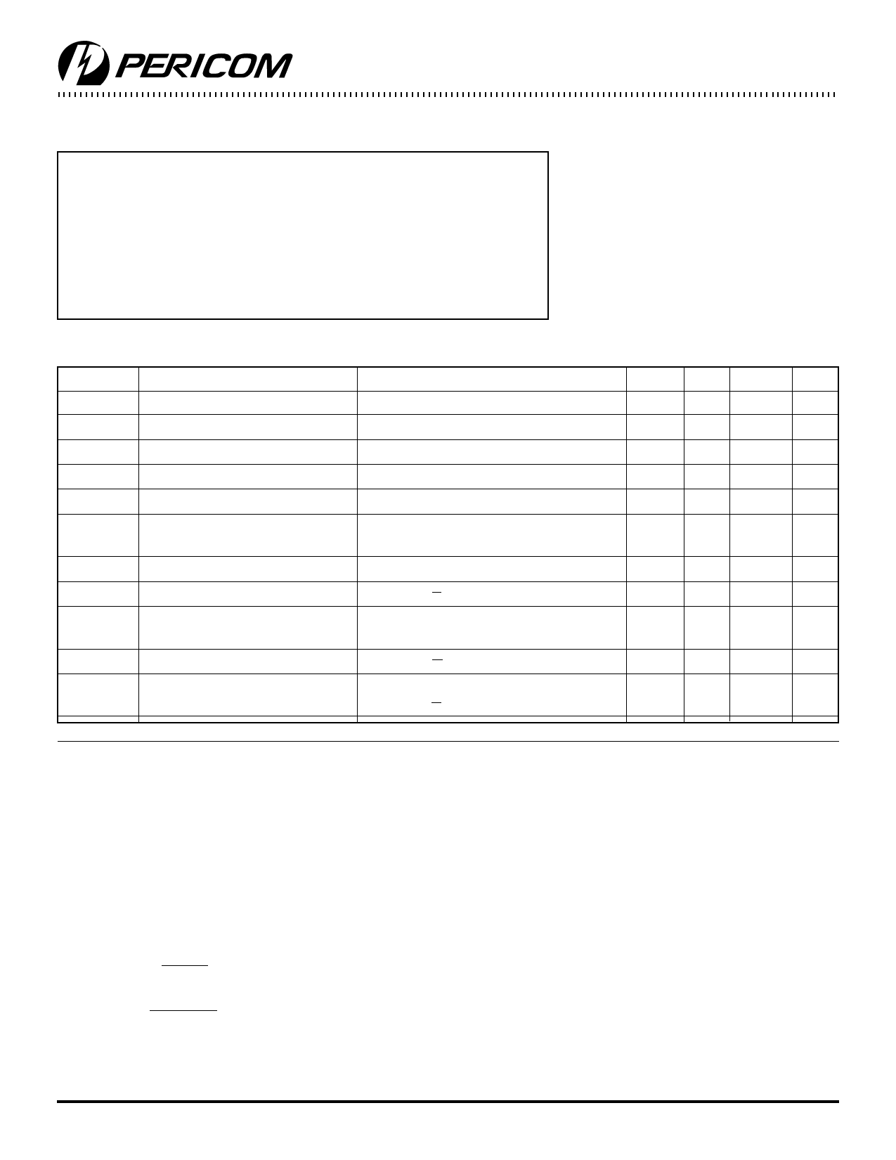
DC Electrical Characteristics (Over the Operating Range, TA = 0°C to +70°C, VCC = 6.2V, + 5%, – 2%)
Parameters Description
Test Conditions(1)
Min. Typ(2)
VIH
Input HIGH Voltage
Guaranteed Logic HIGH Level
2.0 —
VIL
Input LOW Voltage
Guaranteed Logic LOW Level
–0.5 —
IIH
Input HIGH Current
VCC = Max., VIN = VCC
——
IIL
Input LOW Current
VCC = Max., VIN = GND
——
IOZH
High Impedance Output Current 0 ≤ A, B ≤ VCC
——
VIK
Clamp Diode Voltage
VCC = Min., IIN = –18 mA
—
V
IOS
Short Circuit Current(3)
A (B) = 0V, B (A) = VCC
100 —
VH
Input Hysteresis at Control Pins
— 150
VON
Switch On Voltage
VIN = 4.5V, E = LOW
See Figure 10, RL = 100Ω
3.7(4) 4.06(5)
RON(6) M1 Switch On Resistance
Calculated from VON
19 11.2
RON(7) M2 Switch On Resistance
VIN = 4.5V, E = LOW
See Figure 10, RL = 100Ω
2.0 3.0
∆RON On Resistance Match
VIN = 4.5V, E = LOW
— 1.0
Max.
—
0.8
±1
±1
±1
–0.7
—
—
—
—
—
—
Notes:
1. For Max. or Min. conditions, use appropriate value specified under
Electrical Characteristics for the applicable device type.
2. Typical values are at Vcc = 6.2V, TA = 25°C ambient temperature.
3. Not more than one output should be shorted at one time. Duration of the
test should not exceed one second.
4. VON (min) value is at Vcc = 6.1V, TA = 70°C.
5. The expected AC VON value is about 125 mV higher than the DC VON
value using the similar test circuit in Figure 10 with VIN swing from 0.0V
to 4.5V at 10 MHz sine wave.
6. The value of RON of M1 is calculated with the equvalent mathematical
formula of the test circuit in Figure 10.
RON (M1) = VIN – VON
ION
where
ION =
VON
RL + RON (M2)
with RON (M2) = 3 Ohm
7. This parameter is determined by device characterization but is not
production tested.
Units
V
V
µA
µA
µA
–1.2
mA
mV
V
Ω
Ω
Ω
217
PS7031B 04/29/97
Share Link: 