SPX1202 查看數據表(PDF) - Signal Processing Technologies
零件编号
产品描述 (功能)
比赛名单
SPX1202 Datasheet PDF : 12 Pages
| |||
APPLICATION INFORMATION
Output Capacitor
To ensure the stability of the SPX1202, an
output capacitor of at least 10F (tantalum or
ceramic)or 50F (aluminum) is required. The
value may change based on the application
requirements of the output load or temperature
range. The value of ESR can vary based on the
type of capacitor used in the applications. The
recommended value for ESR is 0.5Ω or less. A
larger value of output capacitance (up to 100F)
can improve the load transient response.
SOLDERING METHODS
The SPX1202 SOT-223 package is designed to
be compatible with infrared reflow or vapor-
phase reflow soldering techniques. During sol-
dering, the non-active or mildly active fluxes
may be used. The SPX1202 die is attached to
the heatsink lead which exits opposite the input,
output, and ground pins.
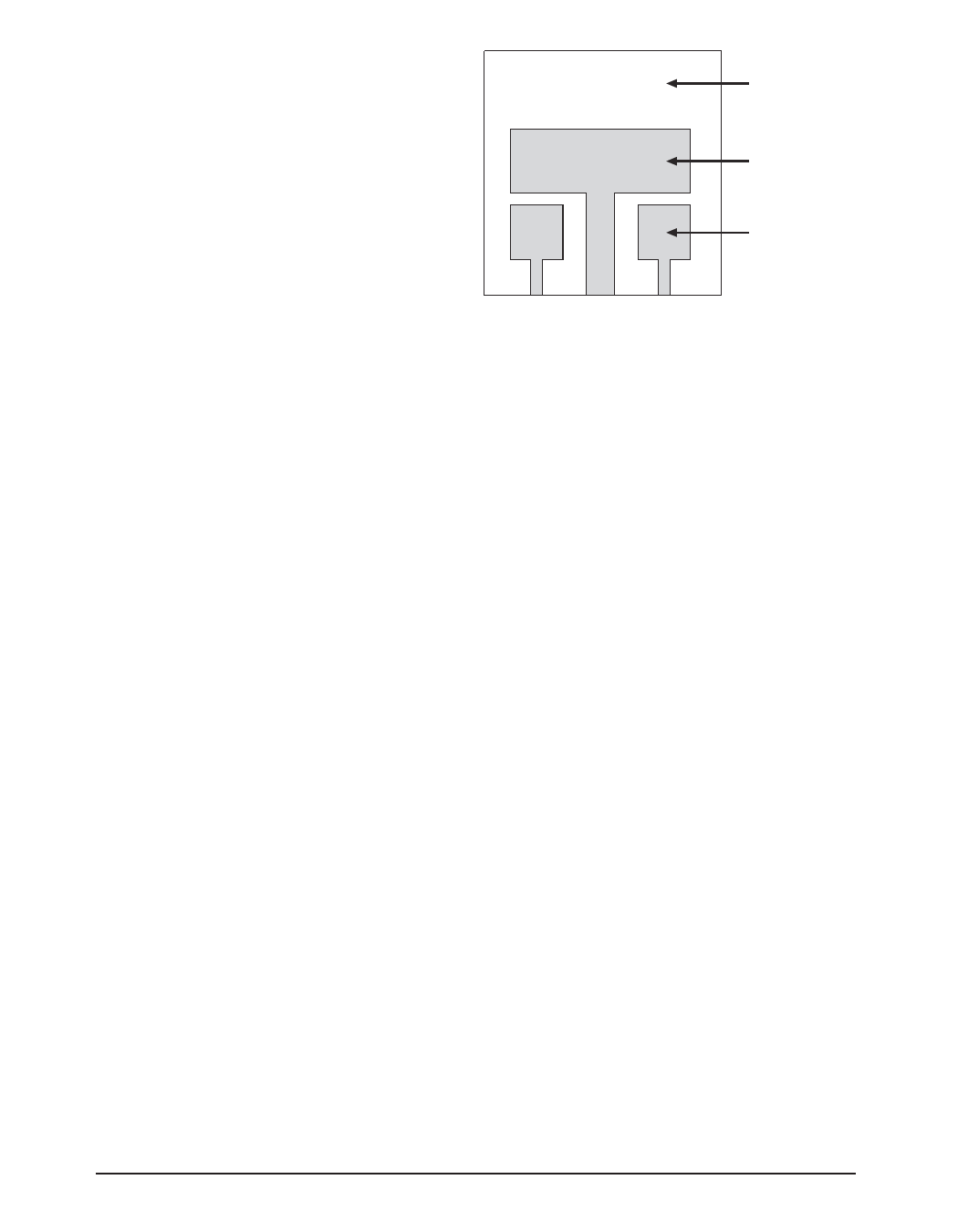
50 X 50mm
35 X 17mm
16 X 10mm
Figure 7. Substrate Layout for SOT-223
in the application can effect the thermal resis-
tance of the SPX1202. The actual thermal resis-
tance can be determined with experimentation.
SPX1202 power dissipation is calculated as
follows:
P = (V - V )(I )
D
IN
OUT OUT
Maximum Junction Temperature range:
Hand soldering and wave soldering should be
avoided since these methods can cause damage
to the device with excessive thermal gradients
on the package. The SOT-223 recommended
soldering method are as follows: vapor phase
reflow and infrared reflow with the component
preheated to within 65C of the soldering tem-
perature range
THERMAL CHARACTERISTICS
The thermal resistance of SPX1202 depends on
the type of package and PC board layout as
shown in Table 1. The SPX1202 features the
internal thermal limiting to protect the device
during overload conditions. Special care needs
to be taken during continuous load conditions
such that the maximum junction temperature
does not exceed 125C. Thermal protection is
activated at >144C and deactiviated at <137C.
Taking the FR-4 printed circuit board and 1/16
thick with 1 ounce copper foil as an experiment,
the PCB material is effective at transmitting
heat with the tab attached to the pad area and a
ground plane layer on the backside of the sub-
strate. Refer to table 1 for the results of the
experiment.
The thermal interaction from other components
TJ= T AMBIENT(max) + P D* (Thermal Resistance)
(Junction-to-ambient)
Maximum junction temperature must not ex-
ceed the 125C.
Ripple Rejection
Ripple rejection can be improved by adding a
capacitor between the ADJ pin and ground as
shown in Figure 7. When ADJ pin bypassing is
used, the value of the output capacitor required
increases to its maximum. If the ADJ pin is not
bypassed, the value of the output capacitor can
be lowered to 10F for an electrolytic aluminum
capacitor or 2.2F for a solid tantalum capacitor
(Fig 10).
However the value of the ADJ-bypass capacitor
should be chosen with respect to the following
equation:
C = 1 / ( 6.28 * F * R )
R
1
Where C = value of the capacitor in Farads
(select an equal or larger standard value),
FR= ripple frequency in Hz,
R1= value of resistor R 1in Ohms.
If an ADJ-bypass capacitor is used, the ampli-
Mar13-07
SPX1202 600 mA Low Dropout Linear Regulator
© 2007 Sipex Corporation
Share Link: 