TA2123AF 查看數據表(PDF) - Toshiba
零件编号
产品描述 (功能)
比赛名单
TA2123AF Datasheet PDF : 20 Pages
| |||
TA2123AF
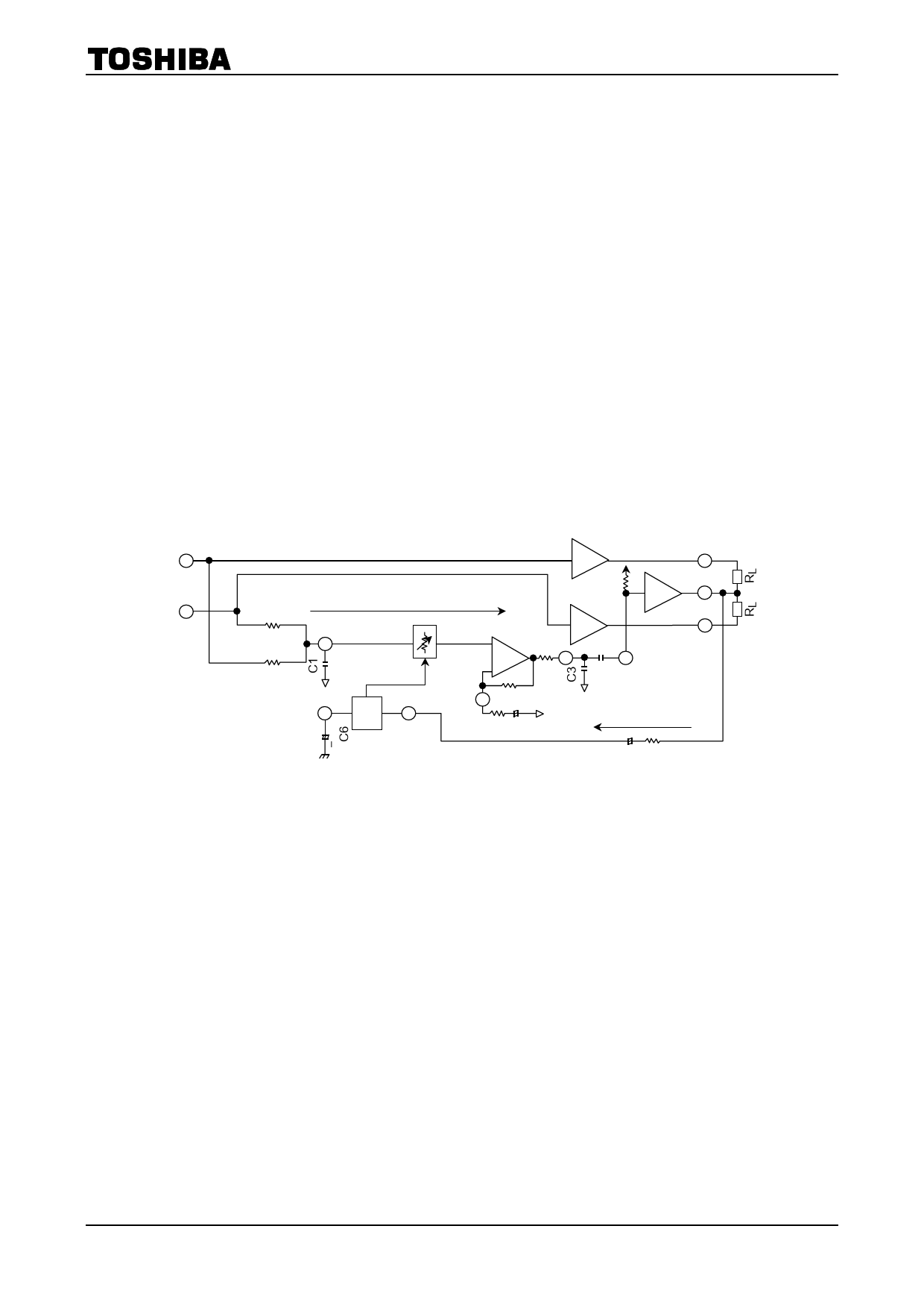
2. Power amplifier stage
(1) Input of power amplifier
Each input signal should be applied through a capacitor. In case that DC current or DC voltage is applied
to each amplifier, the internal circuit has unbalance and the each amplifier doesn’t operate normally.
It is advised that input signal refer to VREF voltage, in order to reduce a pop noise or low frequency leak.
(2) Output application
This IC can chose the output coupling type and OCL type. The C-AMP SW should be connected to GND
in case that the output coupling type is chosen. The supply current decreases when not using the bass
boost function.
(3) Bass boost function
(a) System
This IC has the bass boost function in power amplifier stage. After this system adds the low frequency
ingredient of side amplifier, it is applied into the center amplifier. And the bass boost level is controlled
by the variable impedance circuit (Fig.3)
· Flow of the bass boost signal
Variable impedance circuit→Boost amplifier→Center amplifier
· Flow of the bass boost level
Output of center amplifier→AGC DET (level detection) →
Variable impedance circuit operation
The system of treble boost function is realized by frequency characteristic adjustment of the side
amplifier.
28
PWA
20
Flow of the bass boost signal
PWC
21
27
Ra
ATT
PWB
22
Ra
31
Rd
C4
BST
33
32
36
+
AGC
DET
35
34
Rc
-+
R1 C2
Flow of the Bass boost level
C5 Rb
Fig.3 Bass boost system
9
2002-10-30
Share Link: 