TMC2192KHC 查看數據表(PDF) - Fairchild Semiconductor
零件编号
产品描述 (功能)
比赛名单
TMC2192KHC Datasheet PDF : 69 Pages
| |||
TMC2192
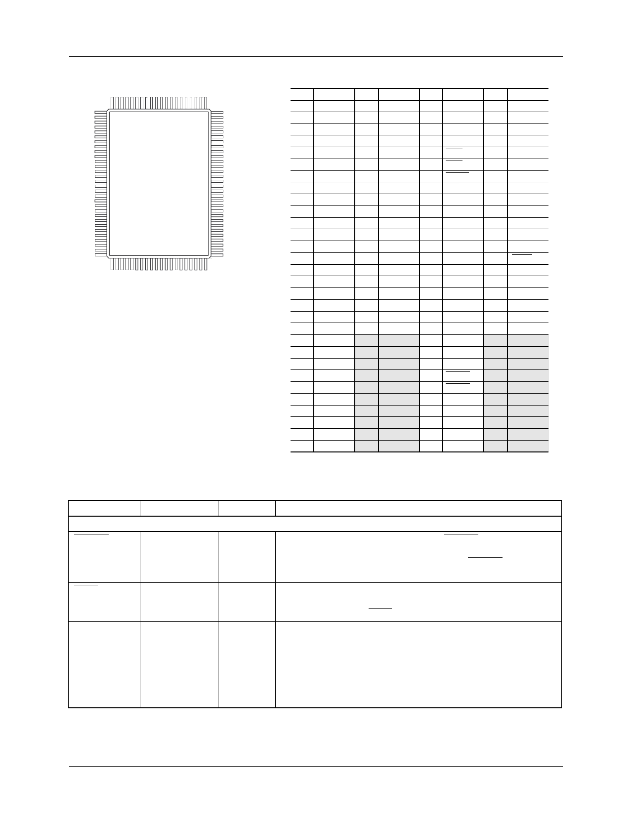
Pin Assignments
100
1
81
80
30
31
51
50
65-6294-14
PRODUCT SPECIFICATION
Pin Function Pin Function Pin Function Pin Function
1
VDDA
31 PD19
2 COMP
32 PD18
3
CBYPCOMP 33 PD17
4
AGND
34 PD16
5
CHROMA 35 PD15
6
CBYPCHROM 36 PD14
7
VDDA
37 PD13
8
RREFCHROM 38 PD12
9
AGND
39 VDD
10 LUMA
40 DGND
11 CBYPLUMA 41 PD11
12 VDDA
42 PD10
13 RREFLUMA 43 PD9
14 AGND
44 PD8
15 AGND
45 PD7
16 VDDA
46 PD6
17 VDDA
47 PD5
18 AGND
48 PD4
19 AGND
49 PD3
20 KEY
50 PD2
21 OL4
22 OL3
23 OL2
24 OL1
25 OL0
26 DGND
27 PD23
28 PD22
29 PD21
30 PD20
51 PD1
81 FLD2
52 PD0
82 FLD1
53 DGND
83 FLD0
54 VDD
84 CVBS9
55 VSIN
85 CVBS8
56 HSIN
86 CVBS7
57 DCVEN 87 CVBS6
58 SER
88 CVBS5
59 CS\/SCL 89 CVBS4
60 R/W\/SDA 90 CVBS3
61 A1/SA1 91 CVBS2
62 A0/SA0 92 CVBS1
63 D7
93 CVBS0
64 D6
94 RESET
65 D5
95 PXCK
66 D4
96 VDD
67 D3
97 DGND
68 D2
98 VREF
69 D1
99 RREFCOMP
70 D0
100 AGND
71 DGND
72 VDD
73 PDC
74 HSOUT
75 VSOUT
76 LINE4
77 LINE3
78 LINE2
79 LINE1
80 LINE0
Pin Definitions
Pin Name
Pin Number
Value Description
CLOCK, SYNC, & CONTROL INPUTS (6 pins)
DCVEN
57
TTL
Digital CVBS Output Enable. When DCVEN is LOW, the
Comp2 output prior to the D/A is routed to D7-0, FLD2-1
providing a digital composite output. When DCVEN is HIGH,
D7-0 and FLD2-1 operate in their normal mode.
HSIN
56
TTL
Horizontal Sync Input. When operating in slave, Genlock, or
DRS-Lock the TMC2192 will start a new horizontal line with
each falling edge of HSIN.
KEY
20
TTL
Hard Key selection. When the control register bit HKEN is set
HIGH and the hardware KEY pin is high, the video data
considered to be the foreground. is routed to the COMP2
output. This control signal is data aligned so that the pixel that is
present on the PD port when KEY signal is latched is at the
midpoint of the key transition. When HKEN is LOW, Key is
ignored.
4
REV. 1.0.0 8/13/03
Share Link: 