UPD4564323 查看數據表(PDF) - NEC => Renesas Technology
零件编号
产品描述 (功能)
比赛名单
UPD4564323 Datasheet PDF : 84 Pages
| |||
µPD4564323 for Rev. E
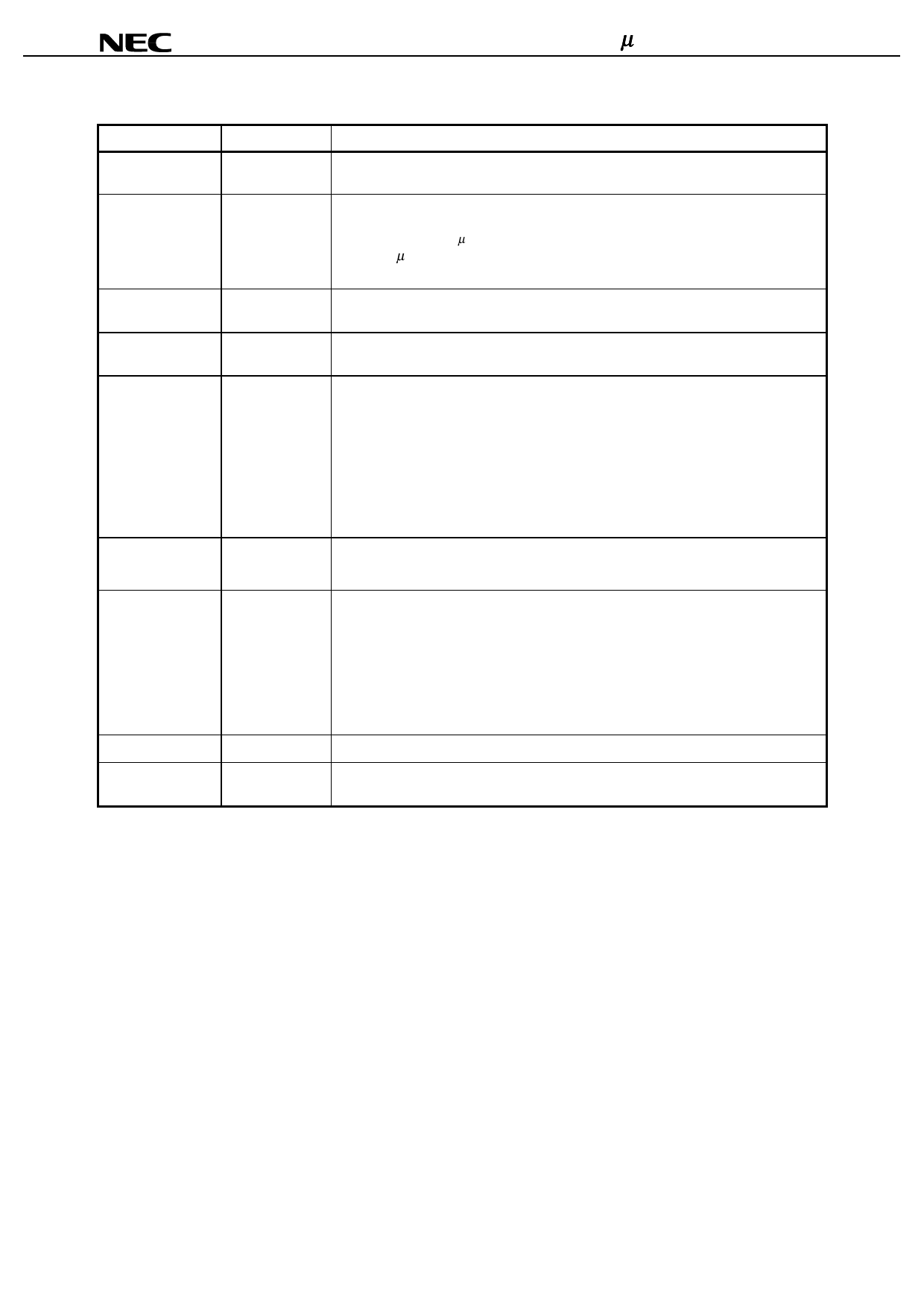
1. Input / Output Pin Function
Pin name
CLK
CKE
/CS
/RAS, /CAS, /WE
A0 - A10
BA0, BA1
DQM0 - DQM3
DQ0 - DQ31
VCC, VSS, VCCQ,
VSSQ
Input / Output
Input
Input
Input
Input
Input
Input
Input
Input / Output
(Power supply)
Function
CLK is the master clock input. Other inputs signals are referenced to the CLK rising
edge.
CKE determine validity of the next CLK (clock). If CKE is high, the next CLK rising
edge is valid; otherwise it is invalid. If the CLK rising edge is invalid, the internal clock
is not issued and the µPD4564323 suspends operation.
When the µPD4564323 is not in burst mode and CKE is negated, the device enters
power down mode. During power down mode, CKE must remain low.
/CS low starts the command input cycle. When /CS is high, commands are ignored
but operations continue.
/RAS, /CAS and /WE have the same symbols on conventional DRAM but different
functions. For details, refer to the command table.
Row Address is determined by A0 - A10 at the CLK (clock) rising edge in the active
command cycle.
Column Address is determined by A0 - A7 at the CLK rising edge in the read or write
command cycle.
A10 defines the precharge mode. When A10 is high in the precharge command cycle,
all banks are precharged; when A10 is low, only the bank selected by BA0 and BA1 is
precharged.
When A10 is high in read or write command cycle, the precharge starts automatically
after the burst access.
BA0 and BA1 are the bank select signal. In command cycle, BA0 and BA1 low select
bank A, BA0 low and BA1 high select bank C, BA0 high and BA1 low select bank B
and then BA0 and BA1 high select bank D.
DQM controls I/O buffers. DQM0 controls DQ0 - DQ7, DQM1 controls DQ8 - DQ15,
DQM2 controls DQ16 - DQ23, DQM3 controls DQ24 - DQ31.
In read mode, DQM controls the output buffers like a conventional /OE pin.
DQM high and DQM low turn the output buffers off and on, respectively.
The DQM latency for the read is two clocks.
In write mode, DQM controls the word mask. Input data is written to the memory cell if
DQM is low but not if DQM is high.
The DQM latency for the write is zero.
DQ pins have the same function as I/O pins on a conventional DRAM.
VCC and VSS are power supply pins for internal circuits. VCCQ and VSSQ are power
supply pins for the output buffers.
8
Data Sheet M14376EJ2V0DS00
Share Link: 