V54C316162V-5 查看數據表(PDF) - Mosel Vitelic, Corp
零件编号
产品描述 (功能)
比赛名单
V54C316162V-5
200/183/166/143 MHz 3.3 VOLT/ 4K REFRESH ULTRA HIGH PERFORMANCE 1M X 16 SDRAM 2 BANKS X 512Kbit X 16
Mosel Vitelic, Corp

V54C316162V-5 Datasheet PDF : 21 Pages
| |||
MOSEL VITELIC
V54C316162V
200/183/166/143 MHz 3.3 VOLT, 4K REFRESH
ULTRA HIGH PERFORMANCE
1M X 16 SDRAM 2 BANKS X 512Kbit X 16
V54C316162V
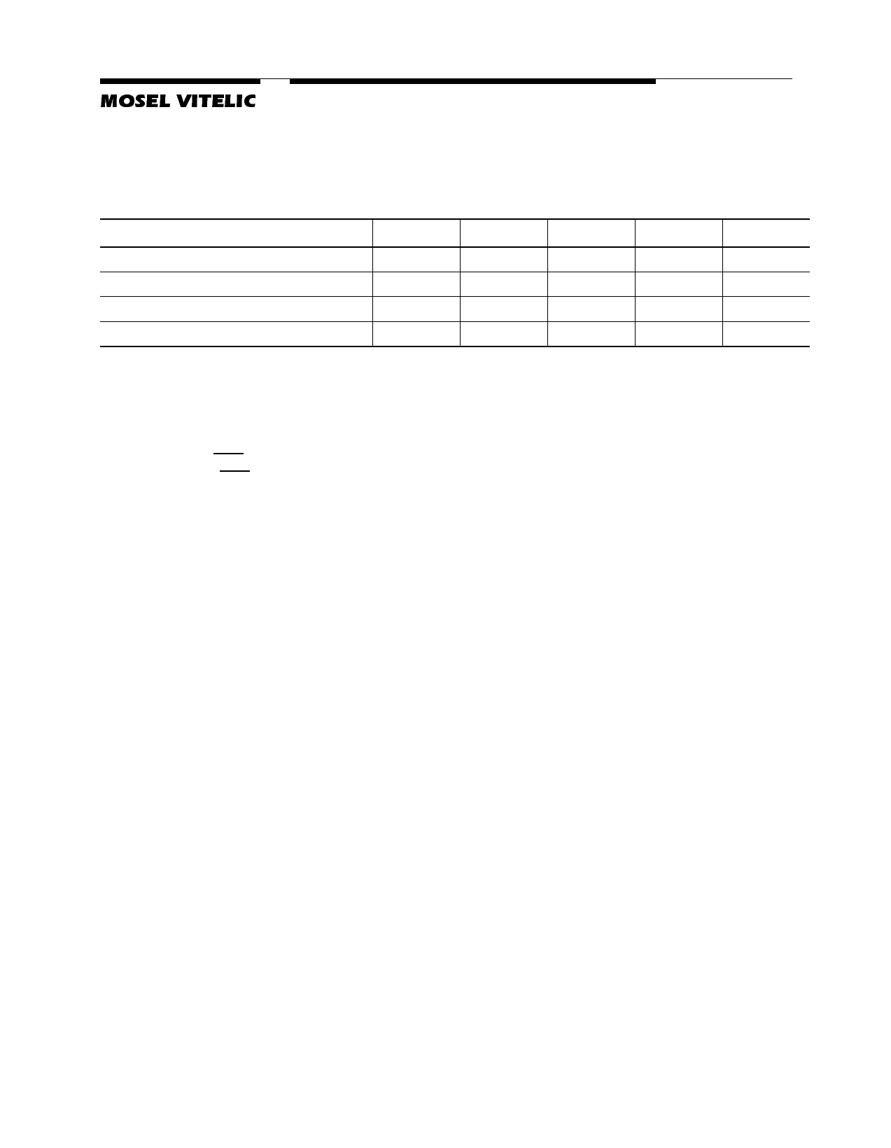
Clock Frequency (tCK)
Latency
Cycle Time (tCK)
Access Time (tAC)
-5
-55
-6
-7
Unit
200
183
166
143
MHz
3
3
3
3
clocks
5
5.5
6
7
ns
5
5.3
5.5
5.5
ns
Features
s JEDEC Standard 3.3V Power Supply
s The V54C316162V is ideally suited for high per-
formance graphics peripheral applications
s Single Pulsed RAS Interface
s Programmable CAS Latency: 2, 3
s All Inputs are sampled at the positive going edge
of clock
s Programmable Wrap Sequence: Sequential or
Interleave
s Programmable Burst Length: 1, 2, 4, 8 and Full
Page for Sequential and 1, 2, 4, 8 for Interleave
s UDQM & LDQM for byte masking
s Auto & Self Refresh
s 4K Refresh Cycles/64 ms
s Burst Read with Single Write Operation
Description
The V54C316162V is a 16,777,216 bits synchro-
nous high data rate DRAM organized as 2 x
524,288 words by 16 bits. The device is designed to
comply with JEDEC standards set for synchronous
DRAM products, both electrically and mechanically.
Synchronous design allows precise cycle control
with the system clock. The CAS latency, burst
length and burst sequence must be programmed
into device prior to access operation.
V54C316162V Rev.2.9 September 2001
1
Share Link: