V62C2804096L-70B 查看數據表(PDF) - Mosel Vitelic, Corp
零件编号
产品描述 (功能)
比赛名单
V62C2804096L-70B Datasheet PDF : 10 Pages
| |||
MOSEL VITELIC
V62C2804096
Pin Descriptions
A0–A18 Address Inputs
These 19 address inputs select one of the 512K x 8
bit segments in the RAM.
CE1, CE2* Chip Enable Inputs
CE1 is active LOW and CE2 is active HIGH. Both
chip enables must be active to read from or write to
the device. If either chip enable is not active, the
device is deselected and is in a standby power
mode. The I/O pins will be in the high-impedance
state when deselected.
OE
Output Enable Input
The Output Enable input is active LOW. With chip
enabled, when OE is LOW and WE HIGH, data of
the selected memory location will be available on
the I/O pins. When OE is HIGH, the I/O pins will be
in the high impedance state.
*CE2 is available on BGA package only.
WE
Write Enable Input
The write enable input is active LOW and controls
read and write operations. With the chip enabled,
when WE is HIGH and OE is LOW, output data will
be present at the I/O pins; when WE is LOW and
OE is HIGH, the data present on the I/O pins will be
written into the selected memory locations.
I/O1–I/O8 Data Input and Data Output Ports
These 8 bidirectional ports are used to read data
from and write data into the RAM.
VCC
GND
Power Supply
Ground
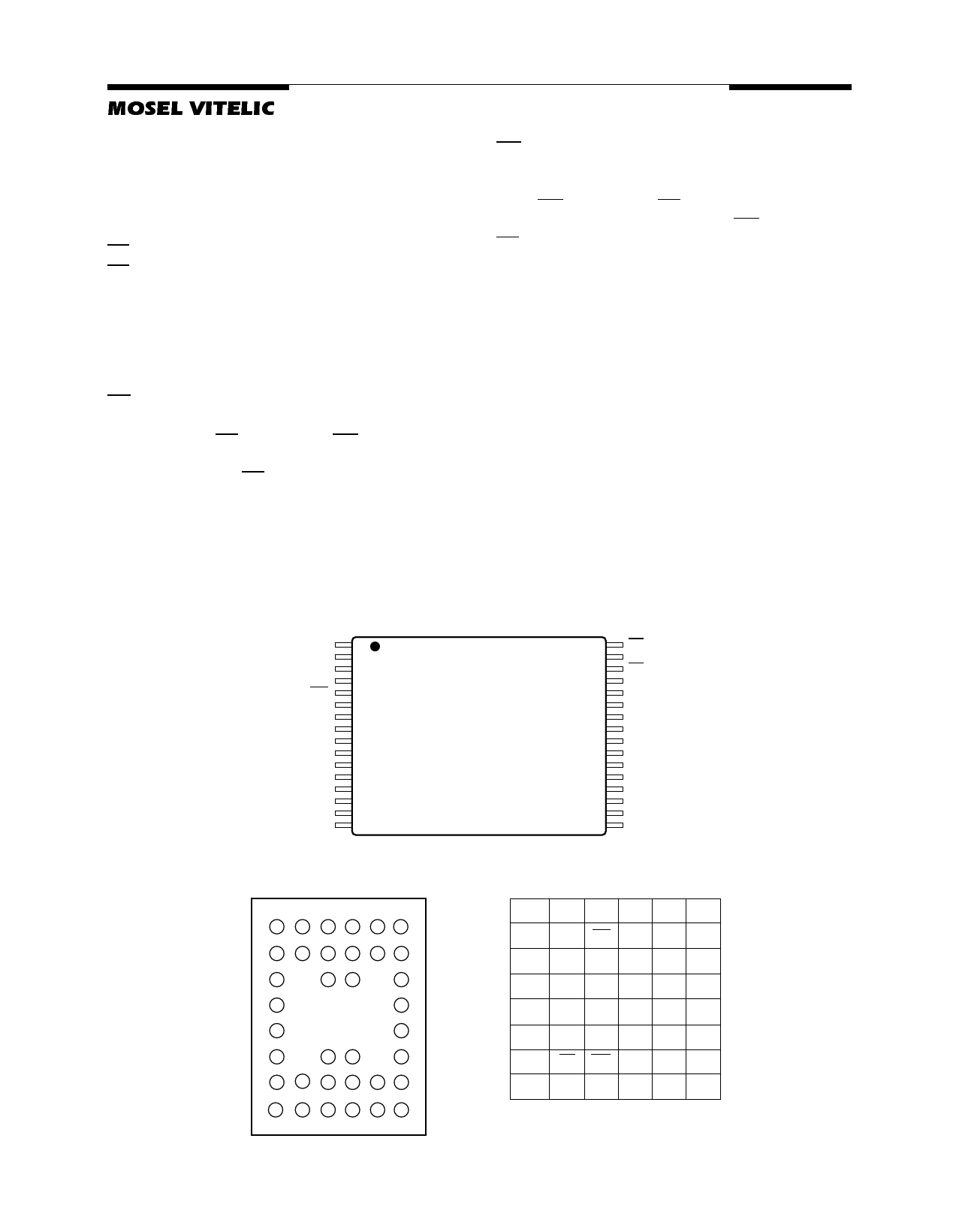
Pin Configurations (Top View)
32-Pin TSOP (Standard)
A11
1
A9
2
A8
3
A13
4
WE
5
A18
6
A15
7
VCC
8
A17
9
A16
10
A14
11
A12
12
A7
13
A6
14
A5
15
A4
16
32
OE
31
A10
30
CE1
29
I/O8
28
I/O7
27
I/O6
26
I/O5
25
I/O4
24
GND
23
I/O3
22
I/O2
21
I/O1
20
A0
19
A1
18
A2
17
A3
1 23456
A
B
C
D
E
F
G
H
TOP VIEW
V62C2804096 Rev. 1.0 November 2001
36 BGA
1
A A0
B I/O5
2
34
A1 CE2 A3
A2 WE A4
56
A6 A8
A7 I/O1
C I/O6 NB NC A5 NB I/O2
D VSS NB NB NB NB VCC
E VCC NB NB NB NB VSS
F I/O7 NB A18 A17 NB I/O3
G I/O8 OE CE1 A16 A15 I/O4
H A9 A10 A11 A12 A13 A14
Note: NC means no connect.
NB means no ball.
TOP VIEW
2
Share Link: 