MAX8662 查看數據表(PDF) - Maxim Integrated
零件编号
产品描述 (功能)
比赛名单
MAX8662 Datasheet PDF : 34 Pages
| |||

Power-Management ICs for
Single-Cell, Li+ Battery-Operated Devices
ABSOLUTE MAXIMUM RATINGS
LX3 to GND ............................................................-0.3V to +33V
DC_ to GND..............................................................-0.3V to +9V
BAT_, CEN, CHG, EN_, PEN_, POK, PV_, PWM,
SYS_, LX1, CS, LX2 to GND .................................-0.3V to +6V
VL to GND ................................................................-0.3V to +4V
BRT, CC3, FB_, IN45, IN67, OVP, REF,
SL_ to GND ...........................................-0.3V to (VSYS + 0.3V)
CT, ISET, PSET, THM to GND .....................-0.3V to (VVL + 0.3V)
OUT4, OUT5 to GND................................-0.3V to (VIN45 + 0.3V)
OUT6, OUT7 to GND................................-0.3V to (VIN67 + 0.3V)
PG_ to GND...........................................................-0.3V to +0.3V
BAT1 + BAT2 Continuous Current ...........................................3A
SYS1 + SYS2 Continuous Current (2 pins) ..............................3A
LX_ Continuous Current ........................................................1.5A
Continuous Power Dissipation (TA = +70°C)
40-Pin 5mm x 5mm TQFN
(derate 35.7mW/°C above +70°C)
(multilayer board) .......................................................2857mW
48-Pin 6mm x 6mm TQFN
(derate 37mW/°C above +70°C) (multilayer board)...2963mW
Operating Temperature Range ..........................-40°C to +85°C
Junction Temperature Range ............................-40°C to +125°C
Storage Temperature Range .............................-65°C to +150°C
Lead Temperature (soldering, 10s) .................................+300°C
Soldering Temperature (reflow) .......................................+260°C
Stresses beyond those listed under “Absolute Maximum Ratings” may cause permanent damage to the device. These are stress ratings only, and functional
operation of the device at these or any other conditions beyond those indicated in the operational sections of the specifications is not implied. Exposure to
absolute maximum rating conditions for extended periods may affect device reliability.
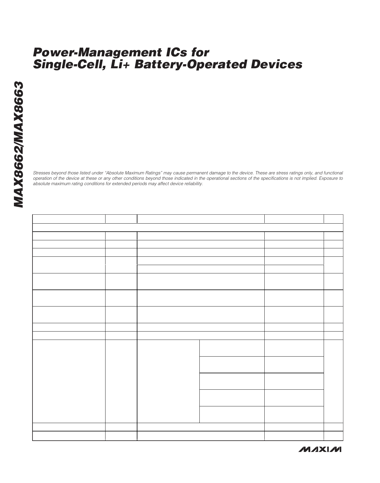
ELECTRICAL CHARACTERISTICS (Input Limiter and Battery Charger)
(VDC = 5V, VBAT = 4V, VCEN = 0V, VPEN_ = 5V, RPSET = 3kΩ, RISET = 3.15kΩ, CCT = 0.068µF, TA = -40°C to +85°C, unless otherwise
noted.) (Note 1)
PARAMETER
INPUT LIMITER
DC Operating Range
DC Undervoltage Threshold
DC Overvoltage Threshold
DC Supply Current
DC Shutdown Current
SYMBOL
CONDITIONS
VDC
VDC_L
VDC_H
(Note 2)
VDC rising, 500mV hysteresis
VDC rising, 100mV hysteresis
ISYS = IBAT = 0mA, VCEN = 0V
ISYS = IBAT = 0mA, VCEN = 5V
VDC = 5V, VCEN = 5V, VPEN1 = VPEN2 = 0V (USB
suspend mode)
MIN TYP MAX UNITS
4.1
8.0
V
3.9 4.0 4.1
V
6.6 6.9 7.2
V
1.5
mA
0.9
110 180 µA
DC-to-SYS Dropout
On-Resistance
RDC_SYS VDC = 5V, ISYS = 400mA, VCEN = 5V
0.1 0.2
Ω
DC-to-BAT Dropout
Threshold
VDR_DC_BAT
When VSYS regulation and charging stops, VDC
falling, 150mV hysteresis
20
50
85
mV
VL Voltage
SYS Regulation Voltage
VVL
IVL = 0 to 10mA
3.1 3.3 3.5
V
VSYS_REG VDC = 5.8V, ISYS = 1mA, VCEN = 5V
5.2 5.3 5.4
V
VPEN1 = 5V, VPEN2 = 5V,
RPSET = 1.5kΩ
1800
2000
2200
DC Input Current Limit
VPEN1 = 5V, VPEN2 = 5V,
RPSET = 3kΩ
900 1000 1100
IDC_LIM
VDC = 5V, VSYS = 4.0V
VPEN1 = 5V, VPEN2 = 5V,
RPSET = 6kΩ
450
500
550
mA
VPEN1 = 0V, VPEN2 = 5V
450 475
500
(500mA USB mode)
PSET Resistance Range
Input Limiter Soft-Start Time
VPEN1 = VPEN2 = 0V
(100mA USB mode)
RPSET Guaranteed by SYS current limit
TSS_DC_SYS Current-limit ramp time
80
90
100
1.5
6.0
kΩ
1.5
ms
2 _______________________________________________________________________________________