UPD72850AGK-9EU 查看數據表(PDF) - NEC => Renesas Technology
零件编号
产品描述 (功能)
比赛名单
UPD72850AGK-9EU Datasheet PDF : 48 Pages
| |||
µPD72850A
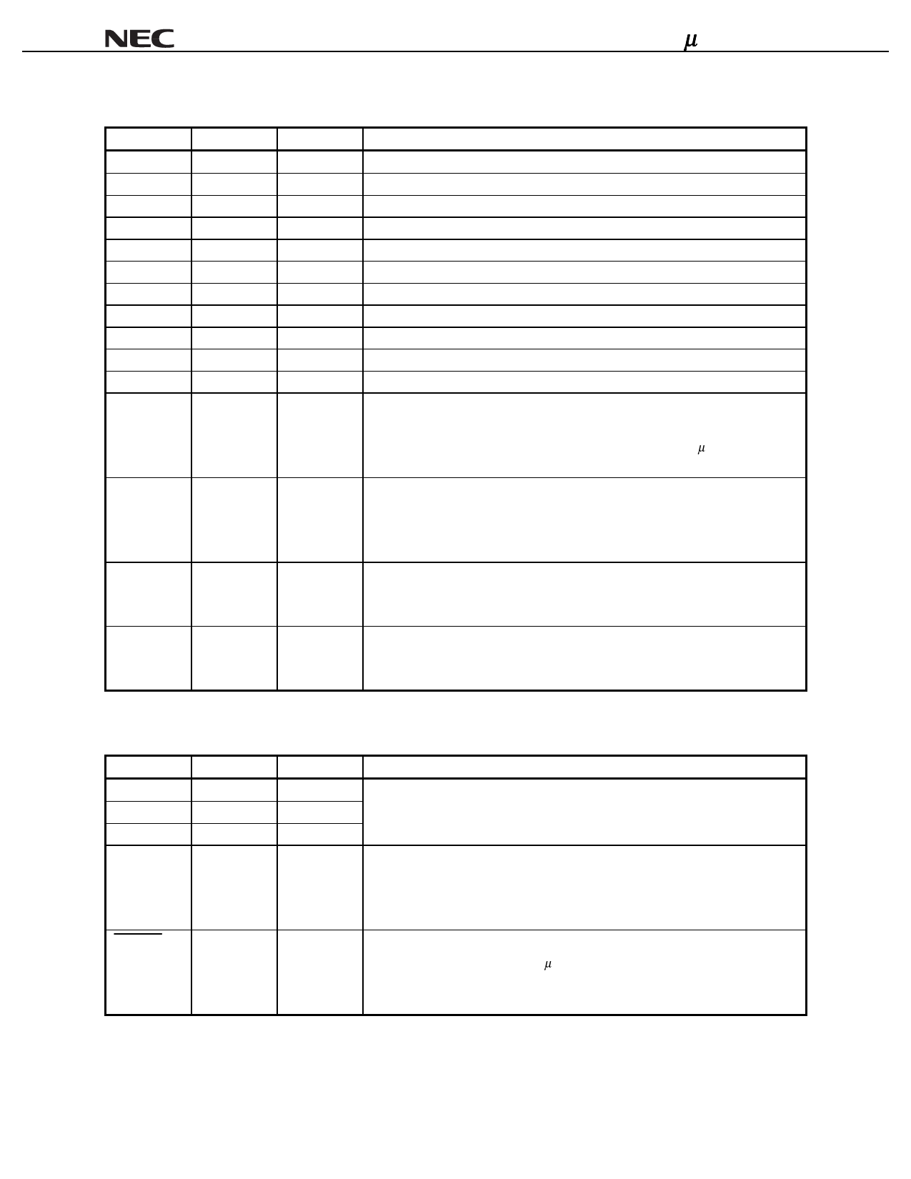
1.2 Link Interface Pins
Name
D0
D1
D2
D3
D4
D5
D6
D7
CTL0
CTL1
LREQ
SCLK
Pin No.
15
16
18
19
21
22
24
25
12
13
6
9
LPS
5
LKON
78
Direct
77
1.3 Control Pins
Name
PC0
PC1
PC2
CMC
Pin No.
2
1
79
3
RESETB
30
I/O
Function
I/O
Data input/output (bit 0)
I/O
Data input/output (bit 1)
I/O
Data input/output (bit 2)
I/O
Data input/output (bit 3)
I/O
Data input/output (bit 4)
I/O
Data input/output (bit 5)
I/O
Data input/output (bit 6)
I/O
Data input/output (bit 7)
I/O
Link interface control (bit 0)
I/O
Llink interface control (bit 1)
I
Link request input
O
Link control output clock
LPS 1: 49.152 MHz output
LPS 0: Clamp to 0 (The clock signal will be output within 25 µsec after change
to “0”)
I
Link power status input
0: Link power off
1: Link power on (PHY/Link direct connection)
Clock signal of about 300 kHz (if isolation)
O
Link-on signal output pin
Link-on signal is 6.144 MHz clock output.
Please refer to 4.2 Link-on Indication.
I
PHY/Link isolation barrier control input
0: Isolation barrier
1: PHY/Link direct connection
I/O
Function
I
Power class set input
I
This pin status will be loaded to Pwr_class bit which allocated to PHY register 4H.
I
IEEE1394-1995 chapter [4.3.4.1]
I
Configuration manager capable setting.
This pin status will be loaded to Contender bit which allocated to PHY register 4H.
0: Non contender
1: Contender
I
Power on reset input.
Connect to DGND through a 0.1 µF capacitor.
0: Reset
1: Normal
8
Data Sheet S14452EJ1V0DS00
Share Link: 