AD7440BRMZ(2015) 查看數據表(PDF) - Analog Devices
零件编号
产品描述 (功能)
比赛名单
AD7440BRMZ
(Rev.:2015)
(Rev.:2015)
Analog Devices

AD7440BRMZ Datasheet PDF : 27 Pages
| |||
AD7440/AD7450A
ABSOLUTE MAXIMUM RATINGS
TA = 25°C, unless otherwise noted.
Table 4.
Parameter
VDD to GND
VIN+ to GND
VIN– to GND
Digital Input Voltage to GND
Digital Output Voltage to GND
VREF to GND
Input Current to Any Pin Except Supplies1
Operating Temperature Range
Commercial (B Version)
Storage Temperature Range
Junction Temperature
θJA Thermal Impedance
MSOP
SOT-23
θJC Thermal Impedance
MSOP
SOT-23
Lead Temperature, Soldering
Vapor Phase (60 sec)
Infrared (15 sec)
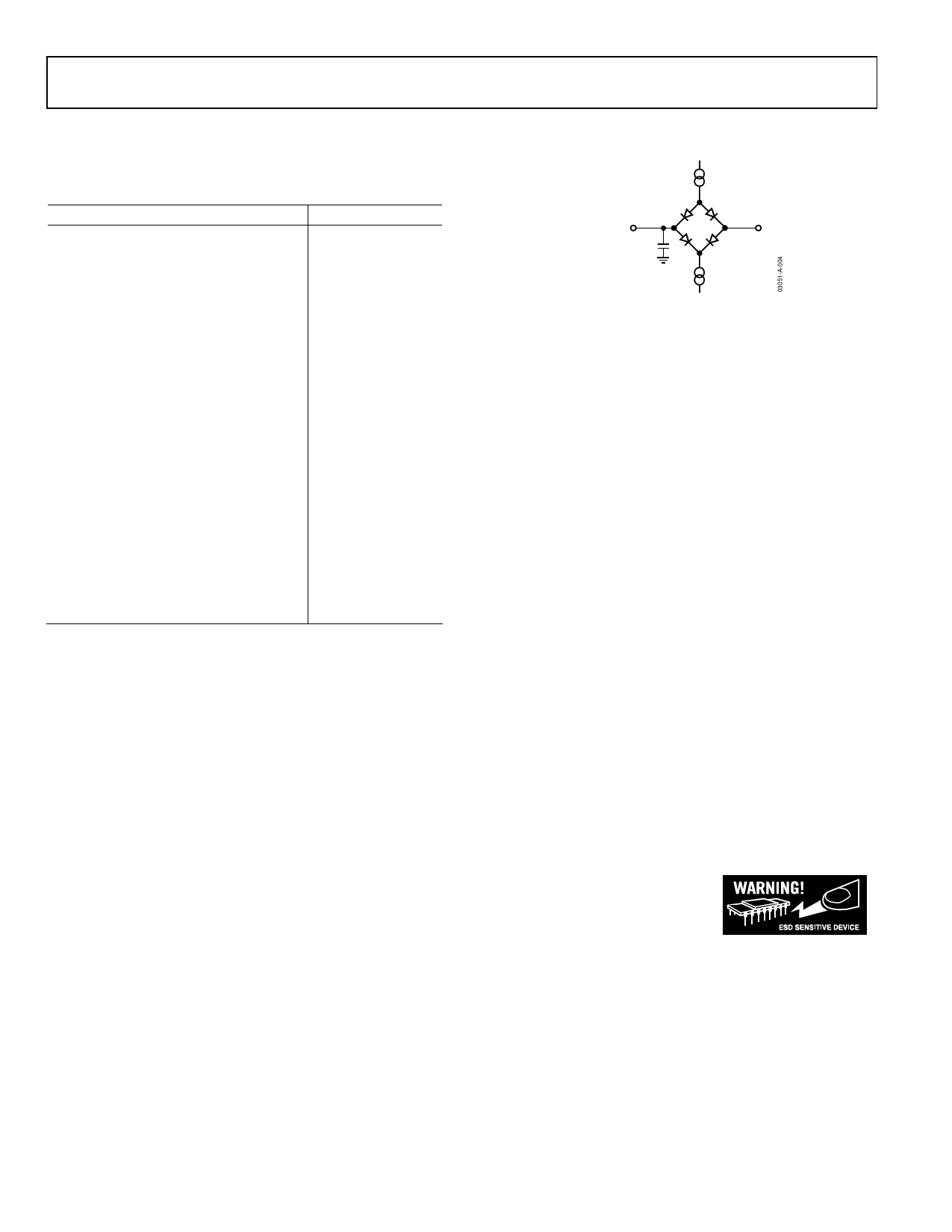
ESD
Rating
–0.3 V to +7 V
–0.3 V to VDD + 0.3 V
–0.3 V to VDD + 0.3 V
–0.3 V to +7 V
–0.3 V to VDD + 0.3 V
–0.3 V to VDD + 0.3 V
±10 mA
–40°C to +85°C
–65°C to +150°C
150°C
205.9°C/W
211.5°C/W
43.74°C/W
91.99°C/W
215°C
220°C
1 kV
1 Transient currents of up to 100 mA do not cause SCR latch up.
Stresses at or above those listed under Absolute Maximum
Ratings may cause permanent damage to the product. This is a
stress rating only; functional operation of the product at these
or any other conditions above those indicated in the operational
section of this specification is not implied. Operation beyond
the maximum operating conditions for extended periods may
affect product reliability.
Data Sheet
1.6mA IOL
TO OUTPUT
PIN CL
25pF
1.6V
200µA IOH
Figure 4. Load Circuit for Digital Output Timing Specifications
ESD CAUTION
Rev. D | Page 8 of 27
Share Link: