AD8155 查看數據表(PDF) - Analog Devices
零件编号
产品描述 (功能)
比赛名单
AD8155 Datasheet PDF : 36 Pages
| |||
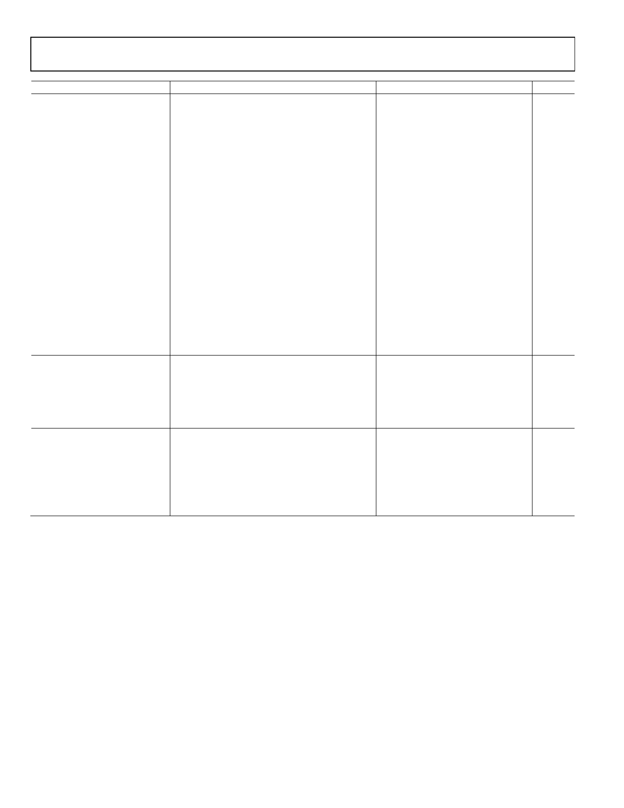
AD8155
Parameter
Supply Current
ICC
VCC = 1.8 V
VCC = 3.3 V
ITTO
VTTO = 1.8 V
VTTO = 3.3 V
ITTI
IDVCC
THERMAL CHARACTERISTICS
Operating Temperature Range
θJA
θJC
Maximum Junction Temperature
LOGIC CHARACTERISTICS4
Input High (VIH)
Input Low (VIL)
Input High (VIH)
Input Low (VIL)
Output High (VOH)
Output Low (VOL)
Conditions
LB_x = 0, PE = 0 dB on all ports, low power mode3
LB_x = 1, PE = 6 dB on all ports, low power mode3
LB_x = 0, PE = 0 dB on all ports, default
LB_x = 1, PE = 6 dB on all ports, default
LB_x = 0, PE = 0 dB on all ports, low power mode3
LB_x = 1, PE = 6 dB on all ports, low power mode3
LB_x = 0, PE = 0 dB on all ports, default
LB_x = 1, PE = 6 dB on all ports, default
LB_x = 0, PE = 0 dB on all ports, low power mode3
LB_x = 1, PE = 6 dB on all ports, low power mode3
LB_x = 0, PE = 0 dB on all ports, default
LB_x = 1, PE = 6 dB on all ports, default
LB_x = 0, PE = 0 dB on all ports, low power mode3
LB_x = 1, PE = 6 dB on all ports, low power mode3
LB_x = 0, PE = 0 dB on all ports, default
LB_x = 1, PE = 6 dB on all ports, default
Still air; JEDEC 4-layer test board, exposed pad
soldered
Still air; thermal resistance through exposed pad
I2C, SDA, SCL, control pins
DVCC = 3.3 V
DVCC = 3.3 V
DVCC = 1.8 V
DVCC = 1.8 V
2 kΩ pull-up resistor to DVCC
IOL = +3 mA
Min
Typ
233
406
350
690
254
435
380
735
66
186
66
183
69
195
69
193
10
2
−40
21.2
1.1
0.7 × DVCC
VEE
VEE
VEE
0.8 × DVCC
0.2 × DVCC
DVCC
Max
Unit
270
mA
480
mA
410
mA
800
mA
300
mA
500
mA
450
mA
850
mA
82
mA
226
mA
82
mA
225
mA
85
mA
230
mA
84
mA
230
mA
20
mA
4
mA
+85
°C
°C/W
°C/W
125
°C
DVCC
V
0.3 × DVCC V
DVCC
V
V
V
0.4
V
1 Bicast is off, loopback is off on all ports, preemphasis is set to minimum on all ports, and equalization is set to minimum on all ports.
2 VICM is the input common-mode voltage.
3 Low power mode is obtained by following the steps identified in the Initialization Sequence for Low Power and LOS_INT Operation section.
4 EQ control pins (EQ_A, EQ_B, EQ_C) require 5 kΩ in series when DVCC > VCC.
Rev. 0 | Page 4 of 36
Share Link: 