BA6780 查看數據表(PDF) - ROHM Semiconductor
零件编号
产品描述 (功能)
比赛名单
BA6780 Datasheet PDF : 14 Pages
| |||
Optical disc ICs
BA6780 / BA6780FP-Y
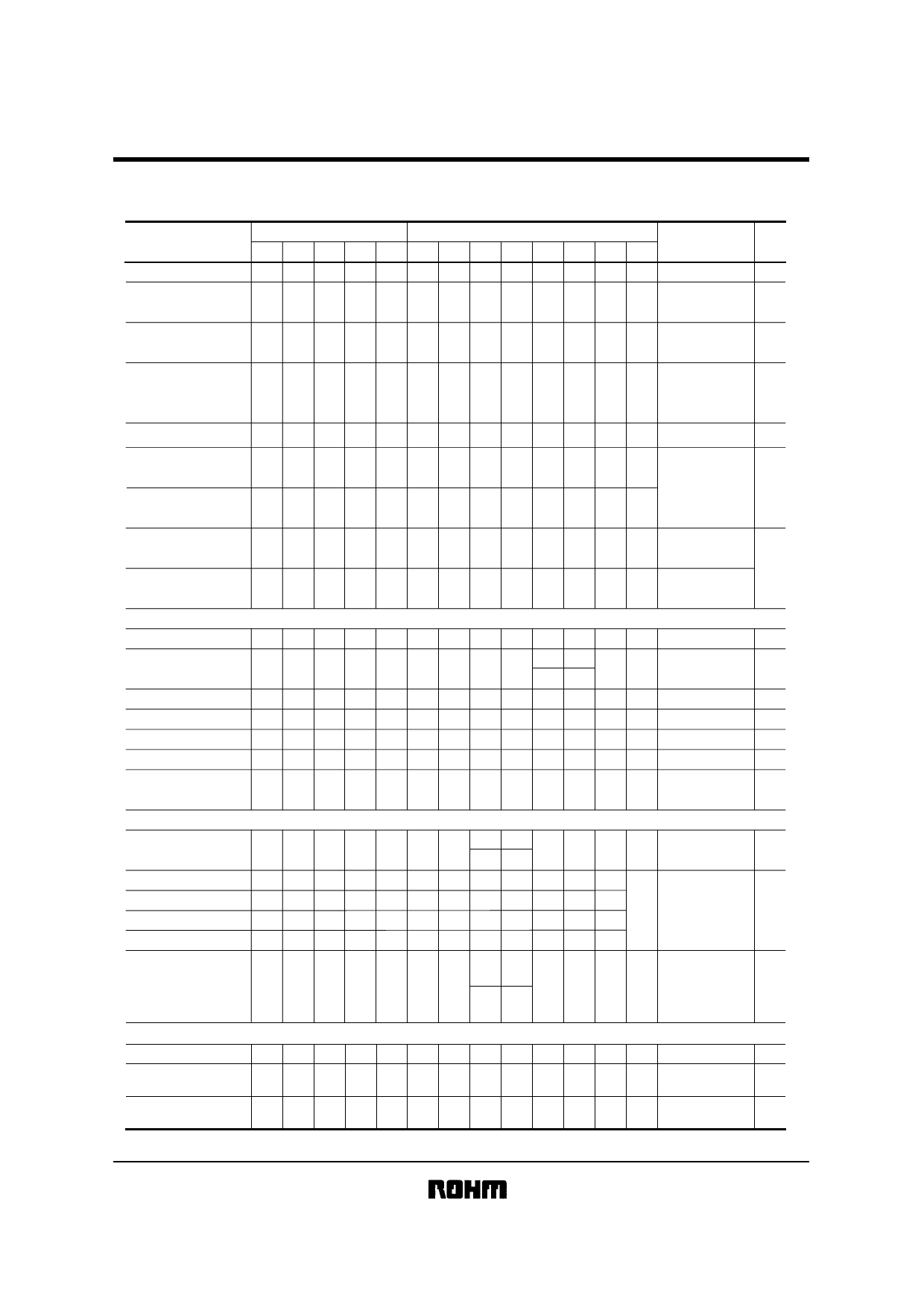
zMeasurement circuit switch table
BA6780 / BA6780FP-Y
Parameter
Quiescent current
SW
Input
SW1 SW2 SW3 SW4 SW5 Vr1 Vr2 F1 R1 F2 R2 VIN IL1
1131 100 00 00−−
Conditions
−
Measure
ment
IQ
Mute on voltage
1
1
3
1
1
2
0
0
5
0
0
−
− VCC swept down VO1
from 10V
Mute off voltage
Vref input voltage
range
Vref pin current
PWM input
high level voltage
PWM input
low level voltage
1
1
3
1
1
2
0
0
5
0
0
−
−
VCC swept up
from 0V
VO1
∗1 Check for
1 1 3 1 2 ∗1 ∗1 0 5 0 5 − −
abnormality in
VO1
output in Vr1 and VO2
Vr2 input range
2231 100 00 00−−
−
II1
II2
1
1
3
1
2
2
2 ∗2 ∗2 ∗2 ∗2
−
− ∗2 Sweep the F/R input, VO1
and check that the mode
1 1 3 1 2 2 2 ∗2 ∗2 ∗2 ∗2 − −
switching is occurring in
a range that satisfies VO2
the rated values
PWM input
high level current
1131 100 55 55−−
−
IF1
IF2
PWM input
low level current
1131 100 55 55−−
−
IR1
IR2
<Electronic governor>
Output offset voltage 1 1 1 1 2 0 0 0 0 5 5 − −
−
VO2
Max. pin-to-pin
output voltage
05
1 1 3 1 204 00
−−
50
−
VO2
Pin-to-pin output voltage 1-1 1 1 1 1 2 0 2.5 0 0 0 5 − −
−
VO2
Pin-to-pin output voltage 1-2 1 1 1 1 2 0 2.5 0 0 5 0 − −
−
VO2
Pin-to-pin output voltage 1-3 1 1 1 1 2 0 2.5 0 0 5 5 − −
−
VO2
Pin-to-pin output voltage 1-4 1 1 1 1 2 0 2.5 0 0 0 0 − −
−
VO2
Voltage gain of positive
feedback amplifier
1
1
2
1
1
0
0
0
0
5
5 ∗3
−
∗3 −20dBV,
1kHz
VO2
<Reversible driver>
Output saturation
voltage
1
1
1
2
1
5
0
0
5
5
0
0
0
−
∗4
∗4 100mA (take care
with polarity)
VCC
−VO1
Pin-to-pin output voltage 2-1 1 1 3 2 1 2.5 0 0 5 0 0 −
Pin-to-pin output voltage 2-2 1
Pin-to-pin output voltage 2-3 1
1
1
3
3
2
1
1 2.5 0
1 2.5 0
5
5
0
5
0
0
0
0
−
∗5 100mA
− ∗5
(take care
with polarity)
VO1
Pin-to-pin output voltage 2-4 1 1 3 1 1 2.5 0 0 0 0 0 −
Output load
fluctuation
05
∗6 Difference in
1 1 3 2 1 2.5 0
0 0 − ∗6
50
output voltage
for I=400mA VO1
and I=100mA
<4.6V constant-voltage output>
Output voltage
1 1 3 1 1 0 0 0 0 0 0 −−
−
Vreg
Output load fluctuation
(source)
1
1
3
1
1
0
0
0
0
0
0
−
− Source Ireg=1mA Vreg
Output load fluctuation
(sink)
1 1 3 1 1 0 0 0 0 0 0 − − Sink Ireg=1mA Vreg
Share Link: 