74ABT16827A(2002) 查看數據表(PDF) - Philips Electronics
零件编号
产品描述 (功能)
比赛名单
74ABT16827A Datasheet PDF : 10 Pages
| |||
Philips Semiconductors
20-bit buffer/line driver, non-inverting (3-State)
Product data
74ABT16827A
74ABTH16827A
FEATURES
• Multiple VCC and GND pins minimize switching noise
• Live insertion/extraction permitted
• 3-State output buffers
• Power-up 3-State
• 74ABTH16827A incorporates bus-hold data inputs which
eliminate the need for external pull-up resistors to hold unused
inputs
• Output capability: +64 mA / –32 mA
• Latch-up protection exceeds 500 mA per Jedec Std 17
• ESD protection exceeds 2000 V per MIL STD 883 Method 3015
and 200 V per Machine Model
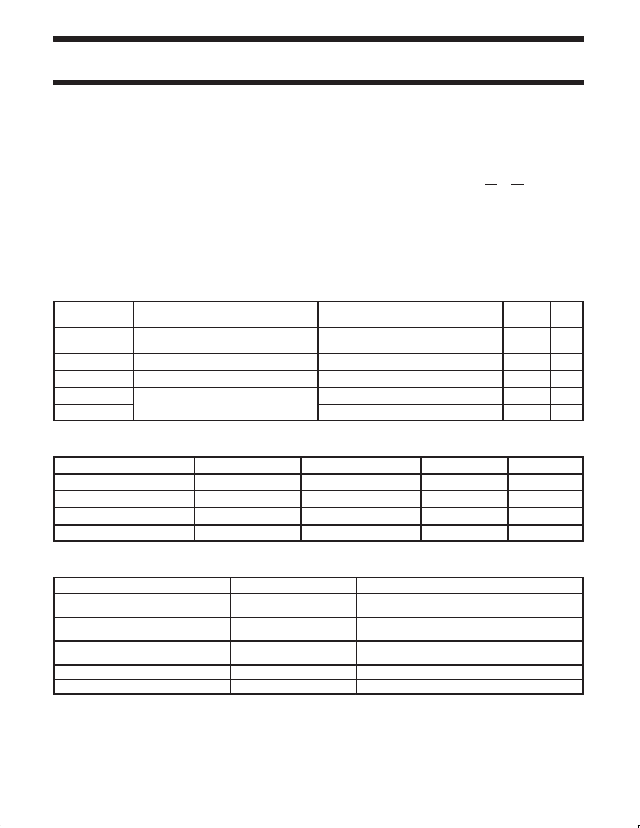
QUICK REFERENCE DATA
SYMBOL
PARAMETER
tPLH
tPHL
CIN
COUT
ICCZ
ICCL
Propagation delay
nAx to nYx
Input capacitance
Output capacitance
Quiescent supply current
DESCRIPTION
The 74ABT16827A high-performance BiCMOS device combines
low static and dynamic power dissipation with high speed and high
output drive.
The 74ABT16827A 20-bit buffers provide high performance bus
interface buffering for wide data/address paths or buses carrying
parity. They have NOR Output Enables (nOE1, nOE2) for maximum
control flexibility.
Two options are available, 74ABT16827A which does not have the
bus-hold feature and 74ABTH16827A which incorporates the
bus-hold feature.
CONDITIONS
Tamb = 25 °C; GND = 0 V
CL = 50 pF; VCC = 5 V
VI = 0 V or VCC
VO = 0 V or VCC; 3-State
Outputs disabled; VCC = 5.5 V
Outputs LOW; VCC = 5.5 V
TYPICAL UNIT
1.7
1.4
ns
4
pF
6
pF
500
µA
9
mA
ORDERING INFORMATION
PACKAGES
56-Pin Plastic SSOP Type III
56-Pin Plastic TSSOP Type II
56-Pin Plastic TSSOP Type II
TEMPERATURE RANGE
–40 °C to +85 °C
–40 °C to +85 °C
–40 °C to +85 °C
PART NUMBER
74ABT16827ADL
74ABT16827ADGG
74ABTH16827ADGG
DWG NUMBER
SOT371-1
SOT364-1
SOT364-1
PIN DESCRIPTION
PIN NUMBER
55, 54, 52, 51, 49, 48, 47, 45, 44, 43,
42, 41, 40, 38, 37, 36, 34, 33, 31, 30
2, 3, 5, 6, 8, 9, 10, 12, 13, 14,
15, 16, 17, 19, 20, 21, 23, 24, 26, 27
1, 56,
28, 29
4, 11, 18, 25, 32, 39, 46, 53
7, 22, 35, 50
SYMBOL
1A0 – 1A9
2A0 – 2A9
1Y0 – 1Y9
2Y0 – 2Y9
1OE0, 1OE1
2OE0, 2OE1
GND
VCC
Data inputs
FUNCTION
Data outputs
Output enable inputs (active-LOW)
Ground (0 V)
Positive supply voltage
2002 Dec 17
2
853-1824 29295
Share Link: 