74AHC595 查看數據表(PDF) - Philips Electronics
零件编号
产品描述 (功能)
比赛名单
74AHC595
Philips Electronics

74AHC595 Datasheet PDF : 20 Pages
| |||
Philips Semiconductors
8-bit serial-in/serial or parallel-out shift
register with output latches; 3-state
Product specification
74AHC595; 74AHCT595
FEATURES
• ESD protection:
HBM EIA/JESD22-A114-A exceeds 2000 V
MM EIA/JESD22-A115-A exceeds 200 V
CDM EIA/JESD22-C101 exceeds 1000 V
• Balanced propagation delays
• All inputs have Schmitt-trigger actions
• Inputs accept voltages higher than VCC
• For AHC only: operates with CMOS input levels
• For AHCT only: operates with TTL input levels
• Specified from −40 to +85 °C and from−40 to +125 °C.
APPLICATIONS
• Serial-to-parallel data conversion
• Remote control holding register.
DESCRIPTION
The 74AHC/AHCT595 are high-speed Si-gate CMOS
devices and are pin compatible with Low power Schottky
TTL (LSTTL). They are specified in compliance with
JEDEC standard No. 7A.
The 74AHC/AHCT595 is an 8-stage serial shift register
with a storage register and 3-state outputs. The shift
register has separate clocks.
Data is shifted on the positive-going transitions of the
SHCP input. The data in each register is transferred to the
storage register on a positive-going transition of the STCP
input. If both clocks are connected together, the shift
register will always be one clock pulse ahead of the
storage register.
The shift register has a serial input (DS) and a serial
standard output (Q7’) for cascading. It is also provided with
asynchronous reset (active LOW) for all 8 shift register
stages. The storage register has 8 parallel 3-state bus
driver outputs. Data in the storage register appears at the
output whenever the output enable input (OE) is LOW.
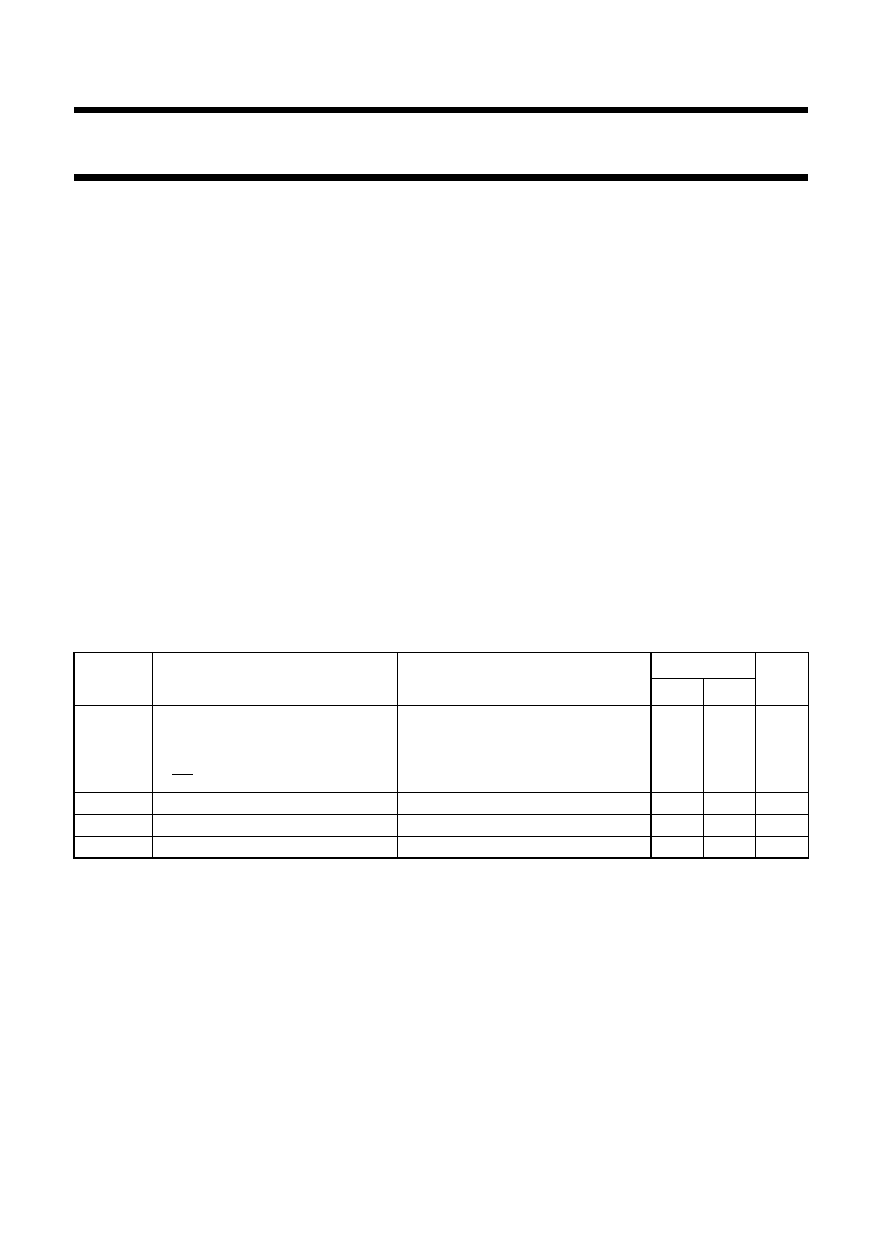
QUICK REFERENCE DATA
GND = 0 V; Tamb = 25 °C; tr = tf ≤ 3.0 ns.
SYMBOL
PARAMETER
CONDITIONS
TYPICAL
UNIT
AHC AHCT
tPHL/tPLH
CI
fmax
CPD
propagation delay
SHCP to Q7’
STCP to Qn
MR to Q7’
input capacitance
maximum clock frequency
power dissipation capacitance
CL = 15 pF; VCC = 5 V
4.0 3.8 ns
4.2 4.0 ns
4.4 4.6 ns
3.0 3.0 pF
170 170 MHz
CL = 50 pF; f = 1 MHz; notes 1, 2 and 3 180 190 pF
Notes
1. CPD is used to determine the dynamic power dissipation (PD in µW).
PD = CPD × VCC2 × fi + ∑ (CL × VCC2 × fo) where:
fi = input frequency in MHz;
fo = output frequency in MHz;
∑ (CL × VCC2 × fo) = sum of outputs;
CL = output load capacitance in pF;
VCC = supply voltage in Volts.
2. The condition is VI = GND to VCC.
3. All 9 outputs switching.
2000 Mar 15
2
Share Link: