74F835 查看數據表(PDF) - Philips Electronics
零件编号
产品描述 (功能)
比赛名单
74F835 Datasheet PDF : 6 Pages
| |||
Philips Semiconductors
8-bit shift register with 2:1 mux-in,
latched “B” inputs, and serial out
Product specification
74F835
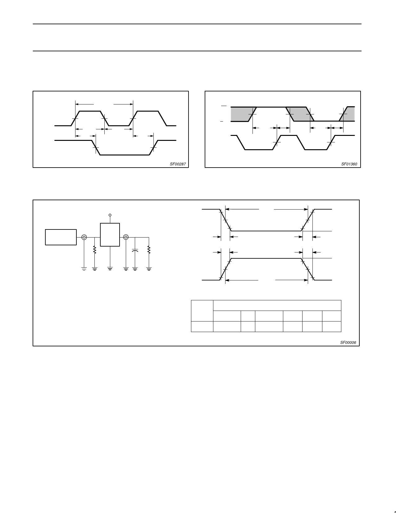
AC WAVEFORMS
For all waveforms, VM = 1.5V.
The shaded areas indicate when the input is permitted to change for predictable output performance.
1/fMAX
CP
VM
VM
VM
tW(H)
tPHL
tW(L)
tPLH
Q7
VM
VM
DS, PE
DnA, DnB
SA/B
CP, LE
VM
ts(H)
VM
th(H)
VM
VM
ts(L)
VM
th(L)
VM
SF00287
Waveform 1. Propagation Delay, Clock Input to Output,
Clock Pulse Width, and Maximum Clock Frequency
SF01360
Waveform 2. Data and Select Setup and Hold Times
TEST CIRCUIT AND WAVEFORMS
VIN
PULSE
GENERATOR
VCC
VOUT
D.U.T.
NEGATIVE
PULSE
90%
tw
VM
10%
tTHL (tf )
VM
10%
tTLH (tr )
90%
AMP (V)
0V
RT
CL RL
Test Circuit for Totem-Pole Outputs
POSITIVE
PULSE
10%
tTLH (tr )
90%
VM
tw
tTHL (tf )
90%
VM
AMP (V)
10%
0V
DEFINITIONS:
RL = Load resistor;
see AC ELECTRICAL CHARACTERISTICS for value.
CL = Load capacitance includes jig and probe capacitance;
see AC ELECTRICAL CHARACTERISTICS for value.
RT = Termination resistance should be equal to ZOUT of
pulse generators.
Input Pulse Definition
family
74F
INPUT PULSE REQUIREMENTS
amplitude VM rep. rate
tw
tTLH
3.0V 1.5V 1MHz 500ns 2.5ns
tTHL
2.5ns
SF00006
1990 Jan 08
6
Share Link: 