74HC595(2017) 查看數據表(PDF) - NXP Semiconductors.
零件编号
产品描述 (功能)
比赛名单
74HC595
(Rev.:2017)
(Rev.:2017)
NXP Semiconductors.

74HC595 Datasheet PDF : 22 Pages
| |||
Nexperia
74HC595; 74HCT595
8-bit serial-in, serial or parallel-out shift register with output latches; 3-state
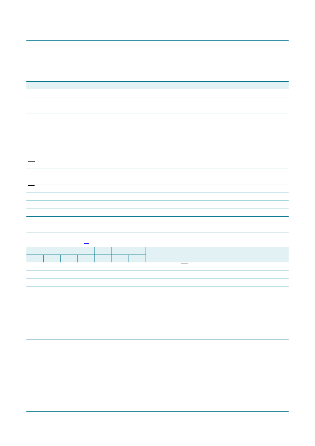
7 Functional description
Table 3. Function table [1]
Control
SHCP STCP OE MR
X
X
L
L
X
↑
L
L
X
X
HL
↑
X
L
H
X
↑
↑
↑
L
H
L
H
Input Output
DS Q7S Qn
X
L
NC
X
L
L
X
L
Z
H
Q6S NC
X
NC QnS
X
Q6S QnS
Function
a LOW-level on MR only affects the shift registers
empty shift register loaded into storage register
shift register clear; parallel outputs in high-impedance OFF-state
logic HIGH-level shifted into shift register stage 0. Contents of all
shift register stages shifted through, e.g. previous state of stage 6
(internal Q6S) appears on the serial output (Q7S).
contents of shift register stages (internal QnS) are transferred to
the storage register and parallel output stages
contents of shift register shifted through; previous contents of the
shift register is transferred to the storage register and the parallel
output stages
[1] H = HIGH voltage state;
L = LOW voltage state;
↑ = LOW-to-HIGH transition;
X = don’t care;
NC = no change;
Z = high-impedance OFF-state.
SHCP
DS
STCP
MR
OE
Q0
Q1
Q6
Q7
Q7S
Figure 7. Timing diagram
Z-state
Z-state
Z-state
Z-state
mna556
74HC_HCT595
Product data sheet
All information provided in this document is subject to legal disclaimers.
Rev. 9 — 28 February 2017
© Nexperia B.V. 2017. All rights reserved.
5 / 22
Share Link: