74HC3G34DC 查看數據表(PDF) - NXP Semiconductors.
零件编号
产品描述 (功能)
比赛名单
74HC3G34DC Datasheet PDF : 13 Pages
| |||
NXP Semiconductors
74HC3G34; 74HCT3G34
Triple buffer gate
Table 8. Dynamic characteristics …continued
Voltages are referenced to GND (ground = 0 V); for test circuit see Figure 6.
Symbol Parameter
Conditions
−40 °C to +85 °C
Min Typ[1] Max
74HCT3G34
tpd
propagation delay nA to nY; see Figure 5
[2]
VCC = 4.5 V
tt
transition time
nY; VCC = 4.5 V; see Figure 5
CPD
power dissipation VI = GND to VCC − 1.5 V
capacitance
-
[3]
-
[4]
-
10
23
6
19
9
-
−40 °C to +125 °C Unit
Min
Max
-
29 ns
-
25 ns
-
-
pF
[1] All typical values are measured at Tamb = 25 °C.
[2] tpd is the same as tPLH and tPHL.
[3] tt is the same as tTLH and tTHL.
[4] CPD is used to determine the dynamic power dissipation (PD in µW).
PD = CPD × VCC2 × fi × N + Σ(CL × VCC2 × fo) where:
fi = input frequency in MHz;
fo = output frequency in MHz;
CL = output load capacitance in pF;
VCC = supply voltage in V;
N = number of inputs switching;
Σ(CL × VCC2 × fo) = sum of outputs.
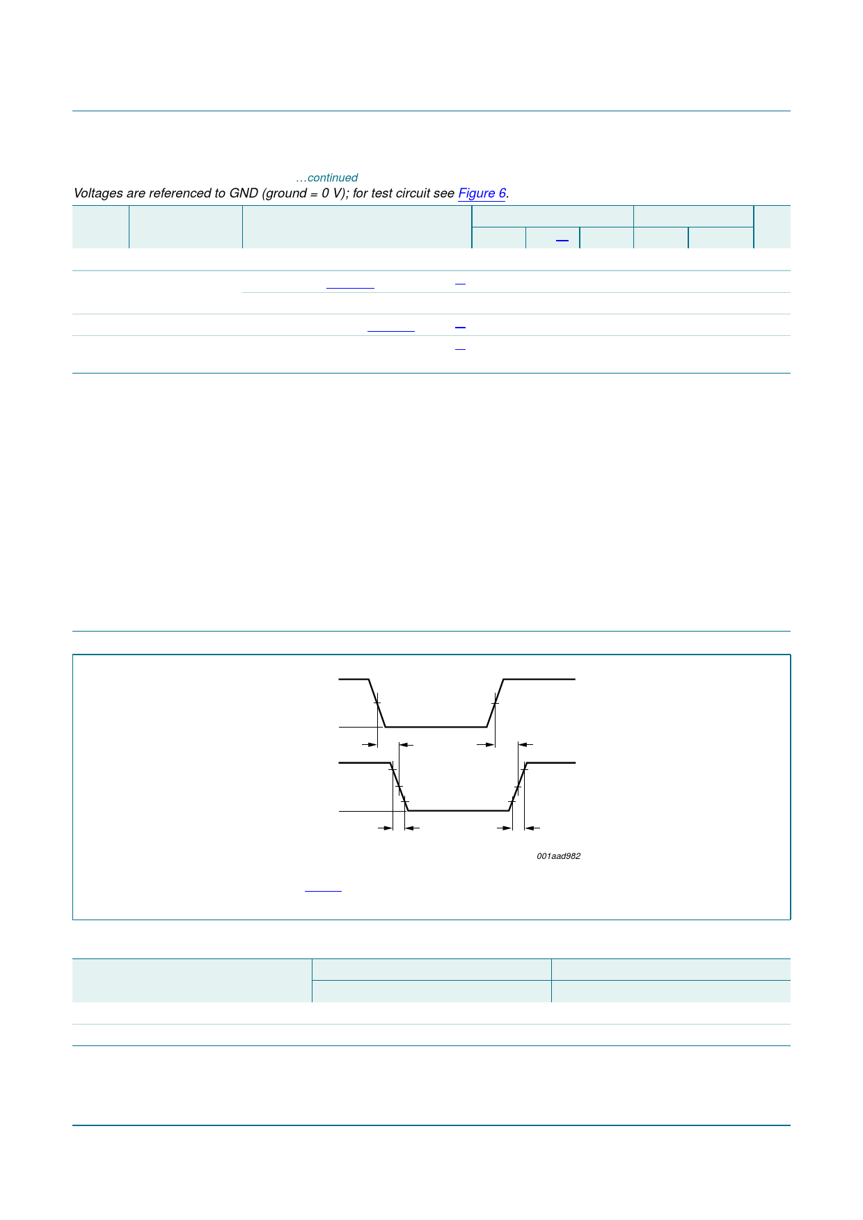
12. Waveforms
VI
input
nA
GND
VOH
output
nY
VOL
VM
t PHL
VM
t THL
VM
VM
10 %
t PLH
90 %
t TLH
001aad982
Measurement points are given in Table 9.
Fig 5. Propagation delay data input (nA) to data output (nY) and transition time output (nY)
Table 9. Measurement points
Type
74HC3G34
74HCT3G34
Input
VM
0.5 × VCC
1.3 V
Output
VM
0.5 × VCC
1.3 V
74HC_HCT3G34_5
Product data sheet
Rev. 05 — 7 May 2009
© NXP B.V. 2009. All rights reserved.
6 of 13
Share Link: 