74LVC544 查看數據表(PDF) - Philips Electronics
零件编号
产品描述 (功能)
比赛名单
74LVC544 Datasheet PDF : 10 Pages
| |||
Philips Semiconductors
Octal D-type registered transceiver, inverting
(3-State)
Product specification
74LVC544A
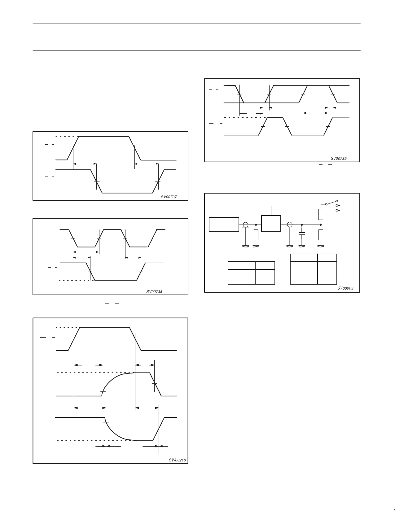
AC WAVEFORMS
VM = 1.5V at VCC w 2.7V
VM = 0.5V * VCC at VCC t 2.7V
VOL and VOH are the typical output voltage drop that occur with the
output load.
VX = VOL + 0.3V at VCC w 2.7V
VX = VOL + 0.1VCC at VCC < 2.7V
VY = VOH – 0.3V at VCC w 2.7V
VY = VOH – 0.1VCC at VCC < 2.7V
VI
An, Bn
INPUT
GND
VOH
Bn, An
OUTPUT
VM
tPHL
VM
tPLH
VOL
SV00737
Figure 1. Input (An, Bn) to output (Bn, An) propagation delays.
VI
LEXX INPUT
GND
VOH
An, Bn
OUTPUT
VOL
VM
VM
tw
tPHL
VM
VM
tPLH
VM
SV00738
Figure 2. Latch enable input (LEXX) pulse width, the latch
enable input to output (An, Bn) propagation delays.
VI
ÉÉÉ An, Bn
INPUT
VM
ÉÉÉÉÉÉ GND
ÉÉÉthÉÉÉÉÉÉÉÉÉÉÉÉÉÉÉÉÉÉÉÉÉth ÉÉÉÉÉÉ
tSU
tSU
VI
LEXX, EXX
INPUT
VM
GND
NOTE: The shaded areas indicate when the input is permitted to change
for predictable output performance.
SV00739
Figure 4. Data set-up and hold times for the (An, Bn) input to
the LEXX and EXX inputs
TEST CIRCUIT
VI
PULSE
GENERATOR
VCC
D.U.T.
RT
VO
CL 50pF
S1
500Ω
2 x VCC
Open
GND
500Ω
VCC
t 2.7V
2.7V – 3.6V
VI
VCC
2.7V
Test
tPLH/tPHL
tPLZ/tPZL
tPHZ/tPZH
S1
Open
2 x VCC
GND
SY00003
Figure 5. Load circuitry for switching times
VI
OEXX, EXX
VM
INPUT
GND
VCC
OUTPUT
LOW-to-OFF
OFF-to-LOW
VOL
tPLZ
VX
tPZL
VM
VOH
OUTPUT
HIGH-to-OFF
OFF-to-HIGH
GND
tPHZ
outputs
enabled
tPZH
VY
outputs
disabled
VM
outputs
enabled
SW00210
Figure 3. 3-State enable and disable times
1998 Jul 29
7
Share Link: 