74LVC594A(2017) 查看數據表(PDF) - NXP Semiconductors.
零件编号
产品描述 (功能)
比赛名单
74LVC594A Datasheet PDF : 21 Pages
| |||
Nexperia
74LVC594A
8-bit shift register with output register
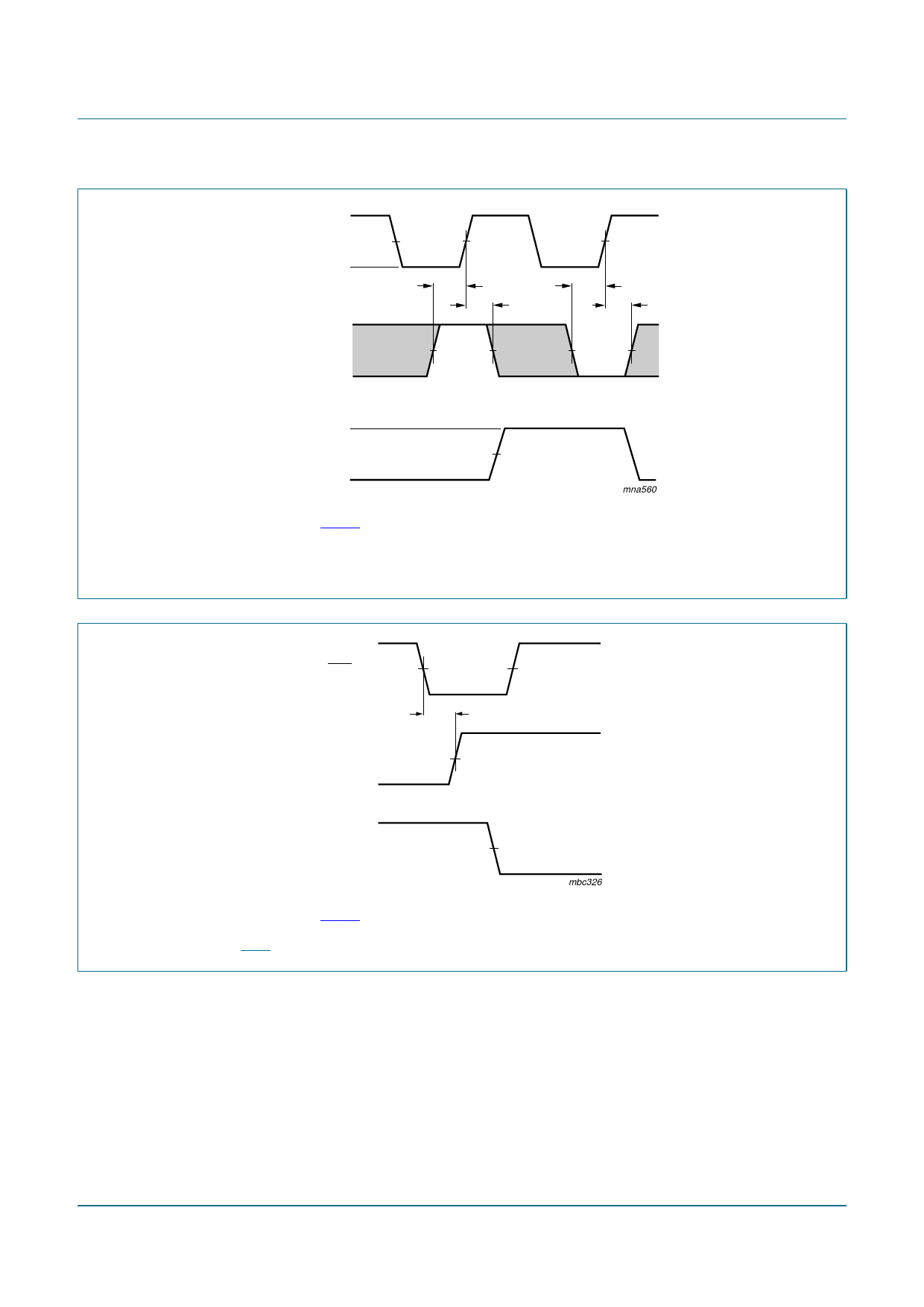
11.1 Waveforms and test circuit
1/ fmax
VI
SHCP input
VM
GND
VOH
tW
t PLH
t PHL
Q7S output
VM
VOL
mna557
Measurement points are given in Table 8.
VOL and VOH are typical output voltage drops that occur with the output load.
Figure 7. The shift clock (SHCP) to serial data output (Q7S) propagation delays, the shift clock pulse width and
maximum shift clock frequency
VI
SHCP input
VM
GND
tsu
VI
1/ fmax
STCP input
VM
GND
VOH
tW
t PLH
t PHL
Qn output
VM
VOL
mna558
Measurement points are given in Table 8.
VOL and VOH are typical output voltage drops that occur with the output load.
Figure 8. The storage clock (STCP) to parallel data output (Qn) propagation delays, the storage clock pulse width
and the shift clock to storage clock set-up time
74LVC594A
Product data sheet
All information provided in this document is subject to legal disclaimers.
Rev. 3 — 20 July 2017
© Nexperia B.V. 2017. All rights reserved.
11 / 21
Share Link: 