GS88237BB-225I 查看數據表(PDF) - Giga Semiconductor
零件编号
产品描述 (功能)
比赛名单
GS88237BB-225I Datasheet PDF : 26 Pages
| |||

Preliminary
GS88237BB-333/300/275/250/225/200
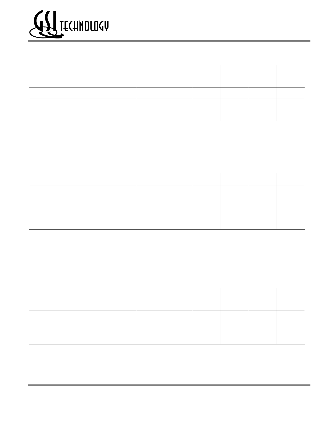
Power Supply Voltage Ranges
Parameter
Symbol Min.
Typ.
Max.
Unit Notes
3.3 V Supply Voltage
VDD3
3.0
3.3
3.6
V
2.5 V Supply Voltage
VDD2
2.3
2.5
2.7
V
3.3 V VDDQ I/O Supply Voltage
VDDQ3
3.0
3.3
3.6
V
2.5 V VDDQ I/O Supply Voltage
VDDQ2
2.3
2.5
2.7
V
Notes:
1. The part numbers of Industrial Temperature Range versions end the character “I”. Unless otherwise noted, all performance specifications quoted are
evaluated for worst case in the temperature range marked on the device.
2. Input Under/overshoot voltage must be –2 V > Vi < VDDn+2 V not to exceed 4.6 V maximum, with a pulse width not to exceed 20% tKC.
VDDQ3 Range Logic Levels
Parameter
Symbol Min.
Typ.
Max.
Unit Notes
VDD Input High Voltage
VIH
2.0
—
VDD + 0.3
V
1
VDD Input Low Voltage
VIL
–0.3
—
0.8
V
1
VDDQ I/O Input High Voltage
VIHQ
2.0
—
VDDQ + 0.3
V
1,3
VDDQ I/O Input Low Voltage
VILQ
–0.3
—
0.8
V
1,3
Notes:
1. The part numbers of Industrial Temperature Range versions end the character “I”. Unless otherwise noted, all performance specifications quoted are
evaluated for worst case in the temperature range marked on the device.
2. Input Under/overshoot voltage must be –2 V > Vi < VDDn+2 V not to exceed 4.6 V maximum, with a pulse width not to exceed 20% tKC.
3. VIHQ (max) is voltage on VDDQ pins plus 0.3 V.
VDDQ2 Range Logic Levels
Parameter
Symbol Min.
Typ.
Max.
Unit Notes
VDD Input High Voltage
VIH
0.6*VDD
—
VDD + 0.3
V
1
VDD Input Low Voltage
VIL
–0.3
—
0.3*VDD
V
1
VDDQ I/O Input High Voltage
VIHQ
0.6*VDD
—
VDDQ + 0.3
V
1,3
VDDQ I/O Input Low Voltage
VILQ
–0.3
—
0.3*VDD
V
1,3
Notes:
1. The part numbers of Industrial Temperature Range versions end the character “I”. Unless otherwise noted, all performance specifications quoted are
evaluated for worst case in the temperature range marked on the device.
2. Input Under/overshoot voltage must be –2 V > Vi < VDDn+2 V not to exceed 4.6 V maximum, with a pulse width not to exceed 20% tKC.
3. VIHQ (max) is voltage on VDDQ pins plus 0.3 V.
Rev: 1.00b 12/2002
11/26
© 2002, Giga Semiconductor, Inc.
Specifications cited are subject to change without notice. For latest documentation see http://www.gsitechnology.com.