AD7457BRT-REEL7(Rev0) 查看數據表(PDF) - Analog Devices
零件编号
产品描述 (功能)
比赛名单
AD7457BRT-REEL7
(Rev.:Rev0)
(Rev.:Rev0)
Analog Devices

AD7457BRT-REEL7 Datasheet PDF : 20 Pages
| |||
AD7457
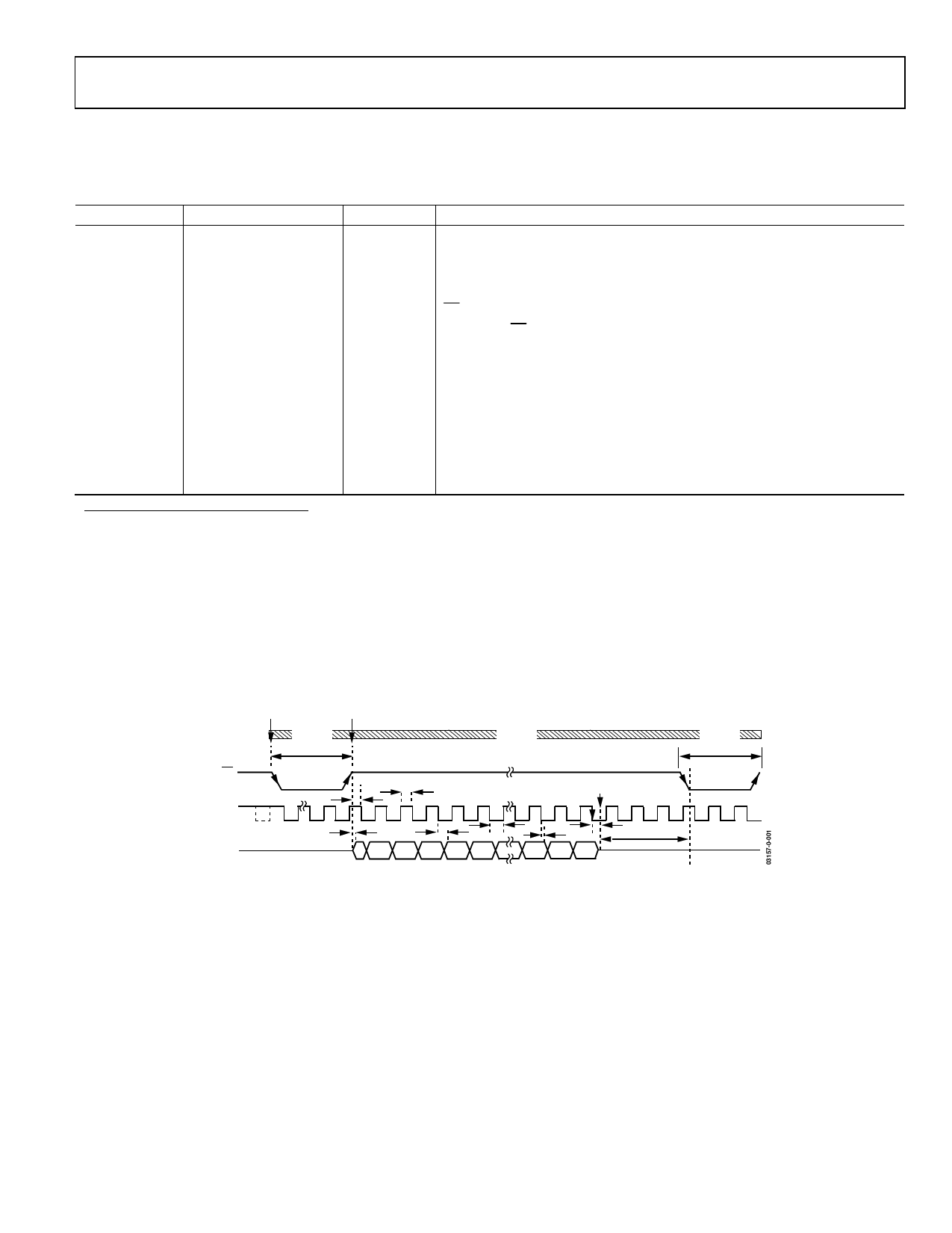
TIMING SPECIFICATIONS1
VDD = 2.7 V to 5.25 V, fSCLK = 10 MHz, fS = 100 kSPS, VREF = 2.5 V, TA = TMIN to TMAX, unless otherwise noted.
Table 2.
Parameter
fSCLK2
tCONVERT
t2
t33
t43
t5
t6
t7
t84
tPOWER-UP5
tPOWER-DOWN
Limit at TMIN, TMAX
10
10
16 × tSCLK
1.6
10
20
40
0.4 tSCLK
0.4 tSCLK
10
10
35
1
7.4
Unit
kHz min
MHz max
µs max
ns min
ns max
ns max
ns min
ns min
ns min
ns min
ns max
µs max
µs min
Description
tSCLK = 1/fSCLK
CS rising edge to SCLK falling edge setup time
Delay from CS rising edge until SDATA three-state disabled
Data access time after SCLK falling edge
SCLK high pulse width
SCLK low pulse width
SCLK edge to data valid hold time
SCLK falling edge to SDATA three-state enabled
SCLK falling edge to SDATA three-state enabled
Power-up time from full power-down
Minimum time spent in power-down
1The timing specifications are guaranteed by characterization. All input signals are specified with tr = tf = 5 ns (10% to 90% of VDD) and timed from a voltage level of
1.6 V. See Figure 2 and the Serial Interface section.
2Mark/space ratio for the SCLK input is 40/60 to 60/40.
3Measured with the load circuit of Figure 3 and defined as the time required for the output to cross 0.8 V or 2.4 V with VDD = 5 V, and the time required for the output to
cross 0.4 V or 2.0 V for VDD = 3 V.
4t8 is derived from the measured time taken by the data outputs to change 0.5 V when loaded with the circuit of Figure 3. The measured number is then extrapolated
back to remove the effects of charging or discharging the 25 pF capacitor. This means that the time, t8, quoted in the timing characteristics, is the true bus relinquish
time of the part and is independent of the bus loading.
5See Power Consumption section.
CS
SCLK
SDATA
POWER
UP
CONVERT
START
TRACK
TPOWERUP
TACQUISITION
t2
t5
HOLD
AUTOMATIC
POWER DOWN
TRACK
TPOWERUP
TACQUISTION
THREE-STATE
t3 t4
t6
00
0
0 DB11 DB10
4 LEADING ZEROS
t8
t7
DB2 DB1 DB0
TPOWERDOWN
THREE-STATE
Figure 2. AD7457 Serial Interface Timing Diagram
Rev. 0 | Page 5 of 20
Share Link: