AD7482ASTZ 查看數據表(PDF) - Analog Devices
零件编号
产品描述 (功能)
比赛名单
AD7482ASTZ Datasheet PDF : 20 Pages
| |||
AD7482
TIMING CHARACTERISTICS
AVDD/DVDD = 5 V ± 5%, AGND = DGND = 0 V, VREF = external; all specifications TMIN to TMAX and valid for VDRIVE = 2.7 V to 5.25 V,
unless otherwise noted.
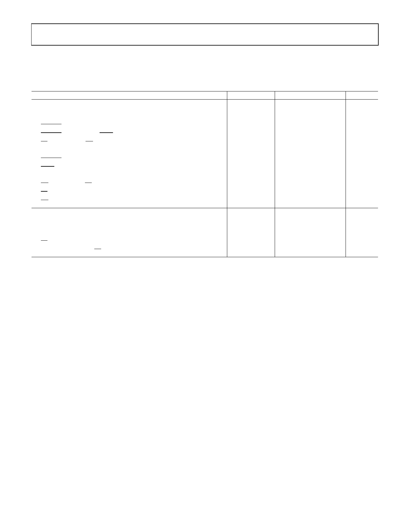
Table 2.
Parameter1
DATA READ
Conversion Time
Quiet Time Before Conversion Start
CONVST Pulse width
CONVST Falling Edge to BUSY Falling Edge
CS Falling Edge to RD Falling Edge
Data Access Time
CONVST Falling Edge to New Data Valid
BUSY Rising Edge to New Data Valid
Bus Relinquish Time
RD Rising Edge to CS Rising Edge
CS Pulse width
RD Pulse width
DATA WRITE
WRITE Pulse Width
Data Setup Time
Data Hold Time
CS Falling Edge to WRITE Falling Edge
WRITE Falling Edge to CS Rising Edge
Symbol
tCONV
tQUIET
t1
t2
t3
t4
t5
t6
t7
t8
t14
t15
t9
t10
t11
t12
t13
Min Typ Max Unit
100
5
0
10
0
30
30
300 ns
ns
100 ns
20
ns
ns
25
ns
30
ns
5
ns
ns
ns
ns
ns
5
ns
2
ns
6
ns
5
ns
0
ns
1 All timing specifications given are with a 25 pF load capacitance. With a load capacitance greater than this value, a digital buffer or latch must be used.
Rev. B | Page 5 of 20
Share Link: 