AD8417 查看數據表(PDF) - Analog Devices
零件编号
产品描述 (功能)
比赛名单
AD8417 Datasheet PDF : 16 Pages
| |||
Data Sheet
0
–50
–100
–150
–200
–250
–300
–350
–400
–450
–500
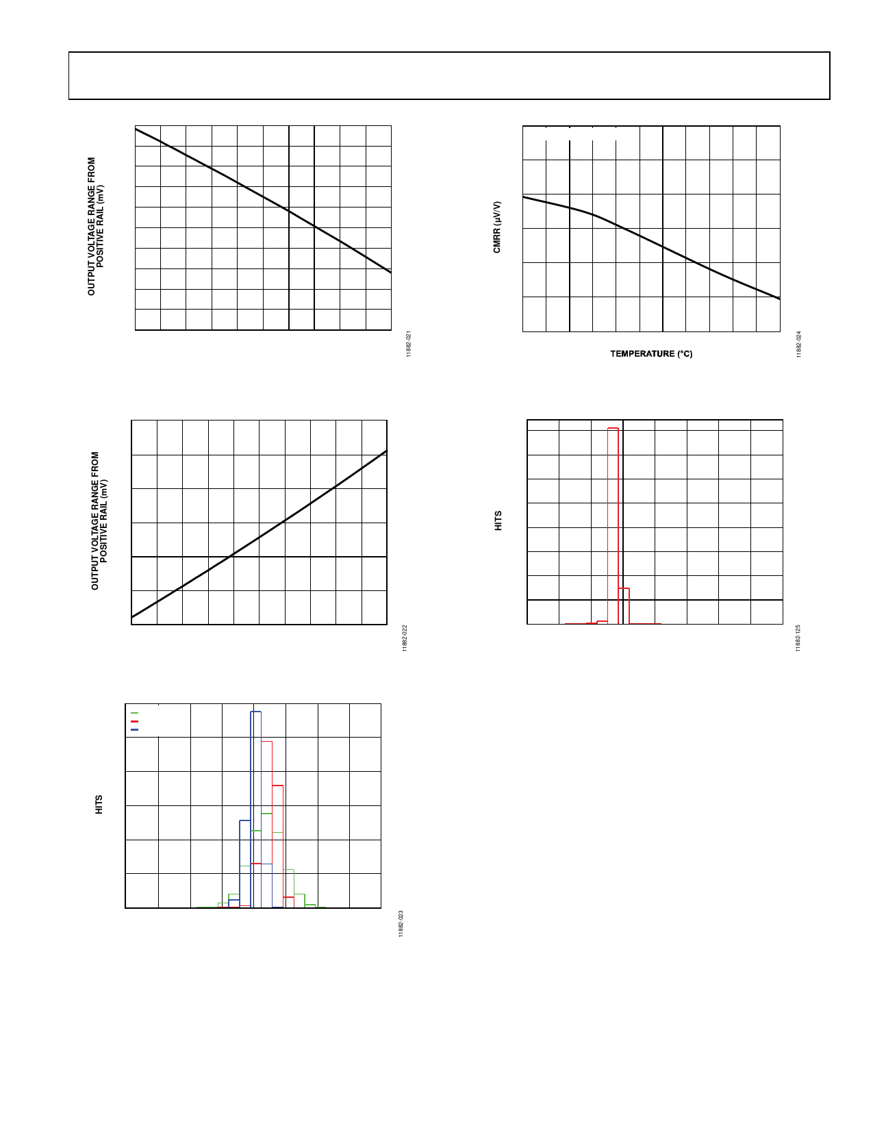
0 1 2 3 4 5 6 7 8 9 10
OUTPUT SOURCE CURRENT (mA)
Figure 21. Output Voltage Range from Positive Rail vs. Output Source Current
300
250
200
150
100
50
0
0 1 2 3 4 5 6 7 8 9 10
OUTPUT SINK CURRENT (mA)
Figure 22. Output Voltage Range from Ground vs. Output Sink Current
1800
1500
–40°C
+25°C
+125°C
1200
900
600
300
0
–400 –300 –200 –100 0
100 200 300 400
VOSI WITH VCC = 5.0V (µV)
Figure 23. Offset Voltage Distribution
AD8417
0.15
NORMALIZED AT 25°C
0.10
0.05
0
–0.05
–0.10
–0.15
–40 –25 –10 5 20 35 50 65 80 95 110 125
Figure 24. CMRR vs. Temperature
2400
2100
1800
1500
1200
900
600
300
0
–8
–6
–4
–2
0
2
4
6
8
GAIN ERROR DRIFT (ppm/°C)
Figure 25. Gain Error Drift Distribution
Rev. 0 | Page 9 of 16
Share Link: 