AD9231 查看數據表(PDF) - Analog Devices
零件编号
产品描述 (功能)
比赛名单
AD9231 Datasheet PDF : 37 Pages
| |||
AD9231
TIMING SPECIFICATIONS
Table 5.
Parameter
Conditions
Min
SYNC TIMING REQUIREMENTS
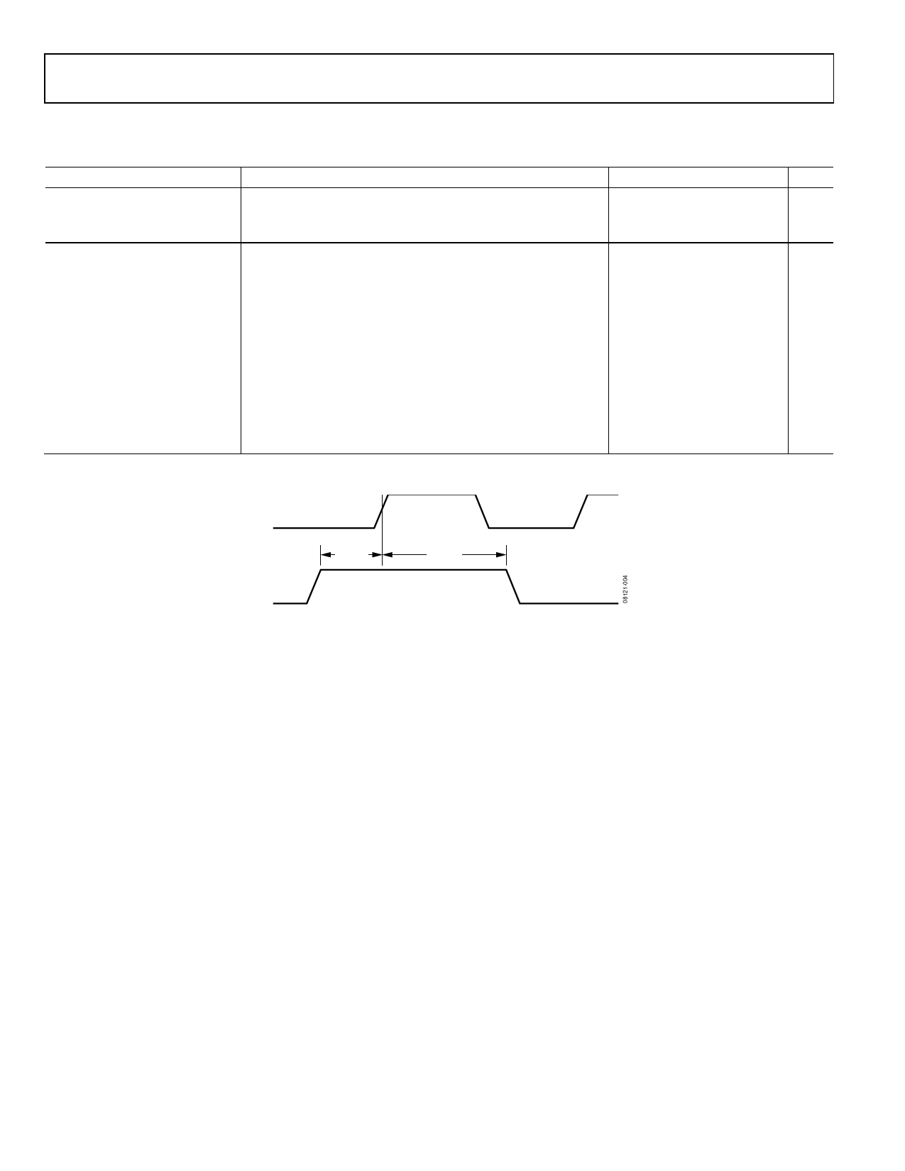
tSSYNC
tHSYNC
SYNC to rising edge of CLK setup time
SYNC to rising edge of CLK hold time
SPI TIMING REQUIREMENTS
tDS
tDH
tCLK
tS
tH
tHIGH
tLOW
tEN_SDIO
Setup time between the data and the rising edge of SCLK
2
Hold time between the data and the rising edge of SCLK
2
Period of the SCLK
40
Setup time between CSB and SCLK
2
Hold time between CSB and SCLK
2
SCLK pulse width high
10
SCLK pulse width low
10
Time required for the SDIO pin to switch from an input to an
10
output relative to the SCLK falling edge
tDIS_SDIO
Time required for the SDIO pin to switch from an output to an
10
input relative to the SCLK rising edge
Data Sheet
Typ
Max Unit
0.24
ns
0.40
ns
ns
ns
ns
ns
ns
ns
ns
ns
ns
CLK+
SYNC
tSSYNC
tHSYNC
Figure 4. SYNC Input Timing Requirements
Rev. B | Page 8 of 36
Share Link: 