P51XAG37KFBD 查看數據表(PDF) - Philips Electronics
零件编号
产品描述 (功能)
比赛名单
P51XAG37KFBD
Philips Electronics

P51XAG37KFBD Datasheet PDF : 34 Pages
| |||
Philips Semiconductors
XA 16-bit microcontroller family
32K/512 OTP/ROM/ROMless, watchdog, 2 UARTs
Product specification
XA-G3
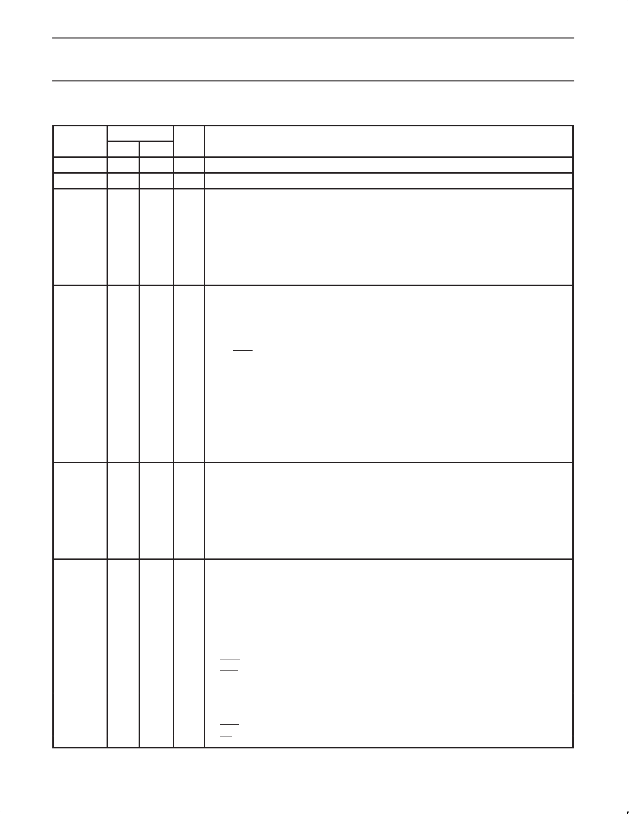
PIN DESCRIPTIONS
PIN. NO.
MNEMONIC
TYPE
PLCC LQFP
NAME AND FUNCTION
VSS
VDD
P0.0 – P0.7
1, 22
23, 44
43–36
16
17
37–30
I Ground: 0V reference.
I Power Supply: This is the power supply voltage for normal, idle, and power down operation.
I/O Port 0: Port 0 is an 8-bit I/O port with a user-configurable output type. Port 0 latches have 1s
written to them and are configured in the quasi-bidirectional mode during reset. The operation of
port 0 pins as inputs and outputs depends upon the port configuration selected. Each port pin is
configured independently. Refer to the section on I/O port configuration and the DC Electrical
Characteristics for details.
When the external program/data bus is used, Port 0 becomes the multiplexed low data/instruction
byte and address lines 4 through 11.
Port 0 also outputs the code bytes during program verification and receives code bytes during
EPROM programming.
P1.0 – P1.7 2–9 40–44, I/O Port 1: Port 1 is an 8-bit I/O port with a user-configurable output type. Port 1 latches have 1s
1–3
written to them and are configured in the quasi-bidirectional mode during reset. The operation of
port 1 pins as inputs and outputs depends upon the port configuration selected. Each port pin is
configured independently. Refer to the section on I/O port configuration and the DC Electrical
Characteristics for details.
Port 1 also provides special functions as described below.
2
40
O
A0/WRH:
Address bit 0 of the external address bus when the external data bus is
configured for an 8 bit width. When the external data bus is configured for a 16
bit width, this pin becomes the high byte write strobe.
3
41
O
A1:
4
42
O
A2:
Address bit 1 of the external address bus.
Address bit 2 of the external address bus.
5
43
O
6
44
I
7
1
O
A3:
RxD1 (P1.4):
TxD1 (P1.5):
Address bit 3 of the external address bus.
Receiver input for serial port 1.
Transmitter output for serial port 1.
8
2
I/O
T2 (P1.6):
Timer/counter 2 external count input/clockout.
9
3
I
T2EX (P1.7): Timer/counter 2 reload/capture/direction control
P2.0 – P2.7 24–31 18–25
I/O Port 2: Port 2 is an 8-bit I/O port with a user-configurable output type. Port 2 latches have 1s
written to them and are configured in the quasi-bidirectional mode during reset. The operation of
port 2 pins as inputs and outputs depends upon the port configuration selected. Each port pin is
configured independently. Refer to the section on I/O port configuration and the DC Electrical
Characteristics for details.
When the external program/data bus is used in 16-bit mode, Port 2 becomes the multiplexed high
data/instruction byte and address lines 12 through 19. When the external program/data bus is used in
8-bit mode, the number of address lines that appear on port 2 is user programmable.
Port 2 also receives the low-order address byte during program memory verification.
P3.0 – P3.7 11,
5,
13–19 7–13
11
5
13
7
14
8
15
9
16
10
17
11
18
12
19
13
I/O Port 3: Port 3 is an 8-bit I/O port with a user configurable output type. Port 3 latches have 1s
written to them and are configured in the quasi-bidirectional mode during reset. the operation of
port 3 pins as inputs and outputs depends upon the port configuration selected. Each port pin is
configured independently. Refer to the section on I/O port configuration and the DC Electrical
Characteristics for details.
Port 3 pins receive the high order address bits during EPROM programming and verification.
Port 3 also provides various special functions as described below.
I
RxD0 (P3.0):
Receiver input for serial port 0.
O
TxD0 (P3.1):
Transmitter output for serial port 0.
I
INT0 (P3.2):
External interrupt 0 input.
I
INT1 (P3.3):
External interrupt 1 input.
I/O
T0 (P3.4):
Timer 0 external input, or timer 0 overflow output.
I/O
T1/BUSW (P3.5): Timer 1 external input, or timer 1 overflow output. The value on this pin is
latched as the external reset input is released and defines the default
external data bus width (BUSW). 0 = 8-bit bus and 1 = 16-bit bus.
O
WRL (P3.6):
External data memory low byte write strobe.
O
RD (P3.7):
External data memory read strobe.
1998 Aug 14
5
Share Link: