ADG508FBNZ 查看數據表(PDF) - Analog Devices
零件编号
产品描述 (功能)
比赛名单
ADG508FBNZ Datasheet PDF : 20 Pages
| |||
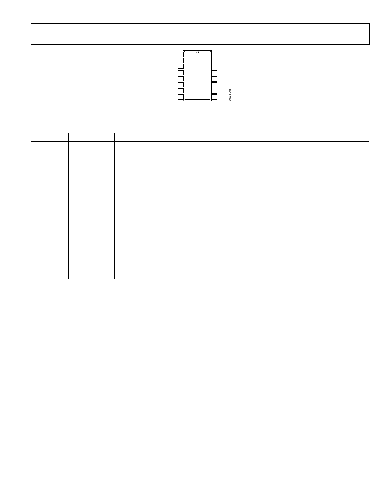
A0 1
16 A1
EN 2
15 GND
VSS 3 ADG509F 14 VDD
S1A 4 TOP VIEW 13 S1B
S2A 5 (Not to Scale) 12 S2B
S3A 6
11 S3B
S4A 7
10 S4B
DA 8
9 DB
Figure 4. ADG509F Pin Configuration
ADG508F/ADG509F
Table 6. ADG509F Pin Function Descriptions
Pin No.
Mnemonic
Description
1
A0
Logic Control Input.
2
EN
Active High Digital Input. When low, the device is disabled and all switches are off. When high,
Ax logic inputs determine on switches.
3
VSS
Most Negative Power Supply Potential. In single-supply applications, this pin can be connected
to ground.
4
S1A
Source Terminal 1A. This pin can be an input or an output.
5
S2A
Source Terminal 2A. This pin can be an input or an output.
6
S3A
Source Terminal 3A. This pin can be an input or an output.
7
S4A
Source Terminal 4A. This pin can be an input or an output.
8
DA
Drain Terminal A. This pin can be an input or an output.
9
DB
Drain Terminal B. This pin can be an input or an output.
10
S4B
Source Terminal 4B. This pin can be an input or an output.
11
S3B
Source Terminal 3B. This pin can be an input or an output.
12
S2B
Source Terminal 2B. This pin can be an input or an output.
13
S1B
Source Terminal 1B. This pin can be an input or an output.
14
VDD
Most Positive Power Supply Potential.
15
GND
Ground (0 V) Reference.
16
A1
Logic Control Input.
Rev. F | Page 7 of 20
Share Link: 