ADN4665 查看數據表(PDF) - Analog Devices
零件编号
产品描述 (功能)
比赛名单
ADN4665 Datasheet PDF : 12 Pages
| |||
ADN4665
TIMING CHARACTERISTICS
VCC = 3.0 V to 3.6 V, RL = 100 Ω, CL1 = 15 pF to GND, all specifications TMIN to TMAX, unless otherwise noted. All typical values are given
for VCC = 3.3 V, TA = 25°C.
Table 2.
Parameter2
Symbol Min Typ
AC CHARACTERISTICS
Differential Propagation Delay, High to Low tPHLD
0.8 1.18
Differential Propagation Delay, Low to High tPLHD
0.8 1.25
Differential Pulse Skew |tPHLD − tPLHD|
tSKD1 5
0
0.07
Channel-to-Channel Skew
tSKD2 6
0
0.1
Differential Part-to-Part Skew
tSKD3 7
0
Differential Part-to-Part Skew
tSKD4 8
0
Rise Time
tTLH
0.38
Fall Time
tTHL
0.4
Disable Time High to Inactive
tPHZ
Disable Time Low to Inactive
tPLZ
Enable Time Inactive to High
tPZH
Enable Time Inactive to Low
Maximum Operating Frequency
tPZL
fMAX 9
200 250
Max Unit
2.0 ns
2.0 ns
0.4 ns
0.5 ns
1.0 ns
1.2 ns
1.5 ns
1.5 ns
5 ns
5 ns
7 ns
7 ns
MHz
Conditions/Comments3, 4
See Figure 3 and Figure 4
See Figure 3 and Figure 4
See Figure 3 and Figure 4
See Figure 3 and Figure 4
See Figure 3 and Figure 4
See Figure 3 and Figure 4
See Figure 3 and Figure 4
See Figure 3 and Figure 4
See Figure 5 and Figure 6
See Figure 5 and Figure 6
See Figure 5 and Figure 6
See Figure 5 and Figure 6
See Figure 5 and Figure 6
1 CL includes probe and jig capacitance.
2 AC parameters are guaranteed by design and characterization.
3 Generator waveform for all tests, unless otherwise specified: f = 50 MHz, ZO = 50 Ω, tr ≤ 1 ns, and tf ≤ 1 ns.
4 All input voltages are for one channel, unless otherwise specified. Other inputs are set to GND.
5 tSKD1 = |tPHLD − tPLHD| is the magnitude difference in differential propagation delay time between the positive-going edge and the negative-going edge of the
same channel.
6 tSKD2 is the differential channel-to-channel skew of any event on the same device.
7 tSKD3, differential part-to-part skew, is defined as the difference between the minimum and maximum specified differential propagation delays. This specification
applies to devices at the same VCC and within 5°C of each other within the operating temperature range.
8 tSKD4, part-to-part skew, is the differential channel-to-channel skew of any event between devices. This specification applies to devices over the recommended operating
temperature and voltage ranges, and across process distribution. tSKD4 is defined as |maximum − minimum| differential propagation delay.
9 fMAX generator input conditions: tr = tf < 1 ns (0% to 100%), 50% duty cycle, 0 V to 3 V. Output criteria: duty cycle = 45% to 55%, VOD > 250 mV, all channels switching.
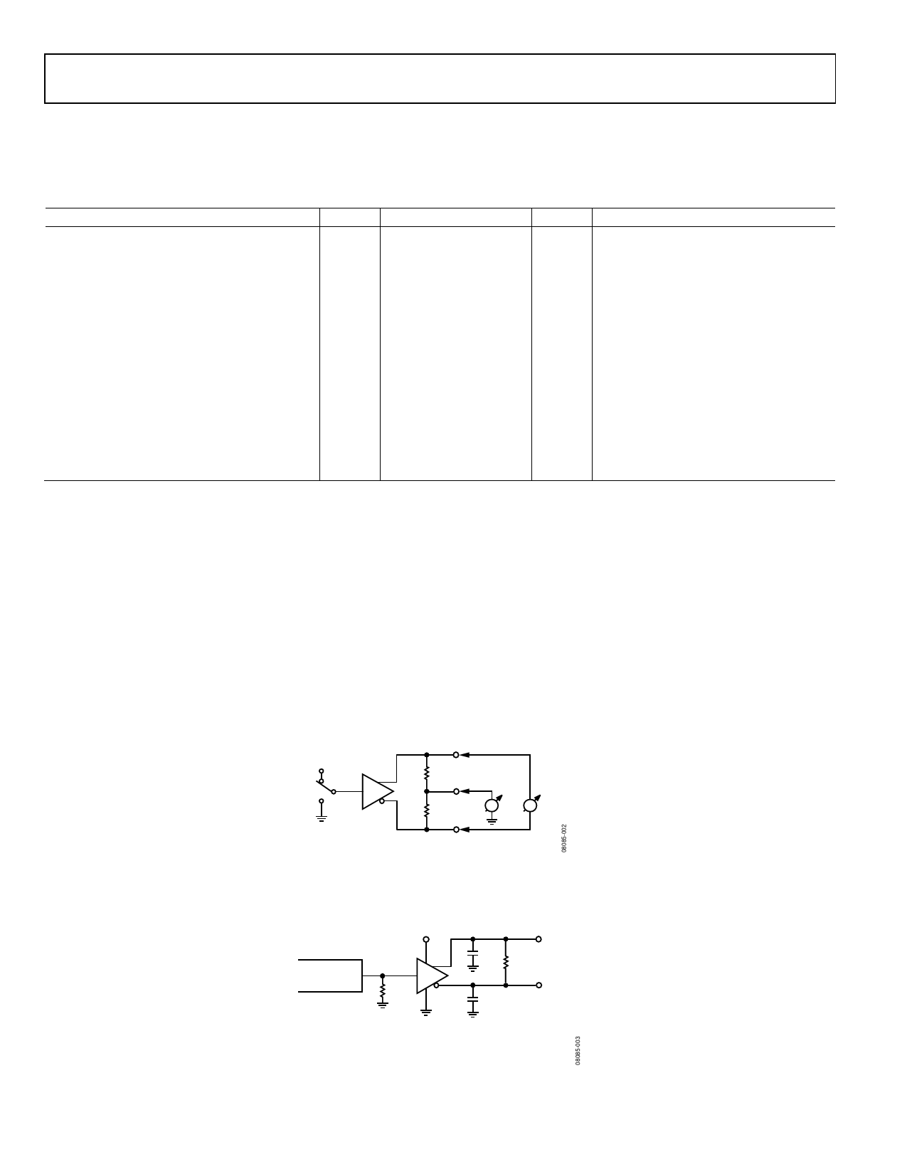
Test Circuits and Timing Diagrams
VCC
DINx
DOUTx+
RL/2
RL/2
V VOS V VOD
DOUTx–
NOTES
1. DRIVER IS ENABLED.
Figure 2. Test Circuit for Driver VOD and VOS
VCC
CL
SIGNAL
GENERATOR
DINx
50Ω
CL
DOUTx+
DOUTx–
DRIVER IS
ENABLED
NOTES
1. CL INCLUDES PROBE AND JIG CAPACITANCE.
Figure 3. Test Circuit for Driver Propagation Delay and Transition Time
Rev. 0 | Page 4 of 12
Share Link: 