ADP2102-EVAL 查看數據表(PDF) - Analog Devices
零件编号
产品描述 (功能)
比赛名单
ADP2102-EVAL Datasheet PDF : 7 Pages
| |||

Preliminary Technical Data
ABSOLUTE MAXIMUM RATINGS
Table 2.
Parameter
AVIN,EN,MODE,FB/OUT to AGND
LX to PGND
PVIN to PGND
PGND to AGND
AVIN to PVIN
Operating Ambient Temperature Range
Operating Junction Temperature
Storage Temperature Range
Soldering Conditions
Rating
−0.3V to +6V
−0.3V to +(VIN + 0.3 V)
−0.3V to +6V
−0.3V to 0.3V
-0.3V to 0.3V
−40°C to +85°C1
125°C
−65°C to +150°C
JEDEC J-STD-020
1 In applications where high power dissipation and poor thermal resistance
are present, the maximum ambient temperature may have to be de-rated.
Maximum ambient temperature (TA(MAX)) is dependent on the maximum
operating junction temperature (TJ(MAXOP)) = 125°C), the maximum power
dissipation of the device (PD(MAX)), and the junction-to-ambient thermal
resistance of the part/package in the application (θJA), using the following
equation: TA(MAX) = TJ(MAXOP) – (θJA x PD(MAX)).
Stresses above those listed under Absolute Maximum Ratings
may cause permanent damage to the device. This is a stress
rating only; functional operation of the device at these or any
other conditions above those indicated in the operational
section of this specification is not implied. Exposure to absolute
maximum rating conditions for extended periods may affect
device reliability.
Absolute maximum ratings apply individually only, not in
combination. Unless otherwise specified all other voltages
referenced to GND.
ADP2102
THERMAL RESISTANCE
Table 3. Thermal Resistance
Package Type
θJA1
8-Lead LFCSP
54
Maximum Power Dissipation
1
Unit
°C/W
W
1 Junction-to-ambient thermal resistance (θJA) of the package is based on
modeling and calculation using a 4-layer board. The junction-to-ambient
thermal resistance is application and board-layout dependent. In
applications where high maximum power dissipation exists, attention to
thermal board design is required. The value of θJA can vary depending on
PCB material, layout, and environmental conditions. For more information,
please refer to Application Note AN-772: A Design and Manufacturing Guide
for the Lead Frame Chip Scale Package (LFCSP).
BOUNDARY CONDITION
Natural convection, 4-layer board, exposed pad soldered to the PCB.
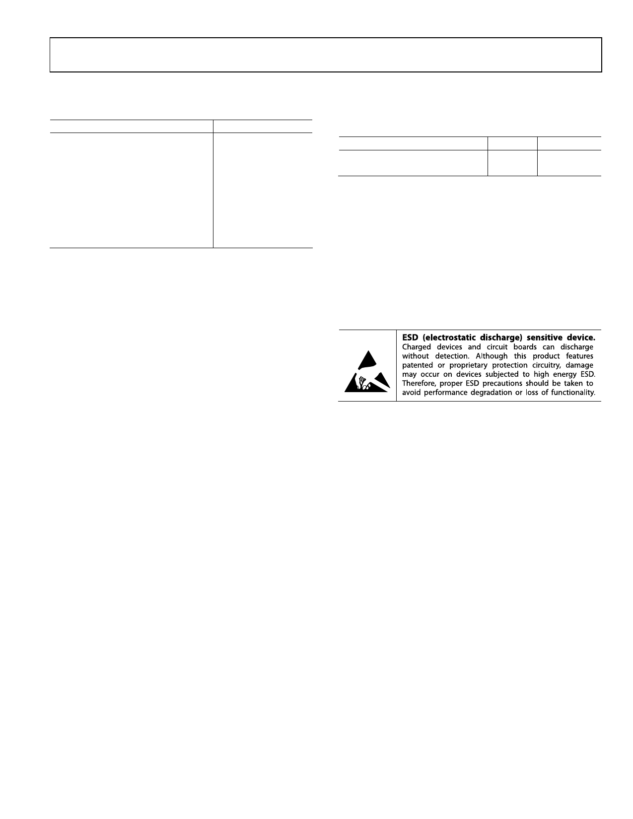
ESD CAUTION
Rev. PrA| Page 3 of 7