AIC1189-12PM3TR 查看數據表(PDF) - Analog Intergrations
零件编号
产品描述 (功能)
比赛名单
AIC1189-12PM3TR Datasheet PDF : 20 Pages
| |||
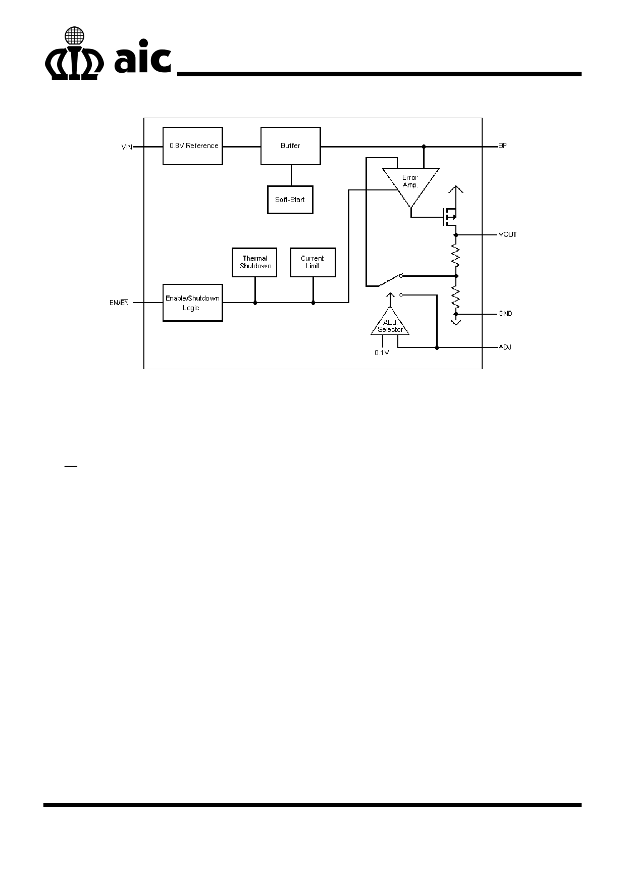
BLOCK DIAGRAM
AIC1189
PIN DESCRIPTION
VIN
– Power supply input pin. Bypass with a 4.7µF capacitor to GND
GND
– Ground.
VOUT
– Regulator Output pin. Sources up to 2A.
EN (5 Pin and 8 Pin) – Chip Enable (Active Low). This pin isn’t allowed to float.
EN (5 Pin and 8 Pin) – Chip Enable (Active High). This pin isn’t allowed to float.
BP (5 Pin and 8 Pin) – Bypass pin. It should be connected to external 22nF capacitor to GND to reduce output
noise. The bypass pin could be floating if it’s unnecessary.
ADJ (5 Pin and 8 Pin) – The output voltage can either be set by the internal feedback resistors when this pin is
grounded, or be set by the external feedback resistors when using a resistive divider.
12
Share Link: 