AIC1190-27PY3R 查看數據表(PDF) - Analog Intergrations
零件编号
产品描述 (功能)
比赛名单
AIC1190-27PY3R Datasheet PDF : 19 Pages
| |||
AIC1190
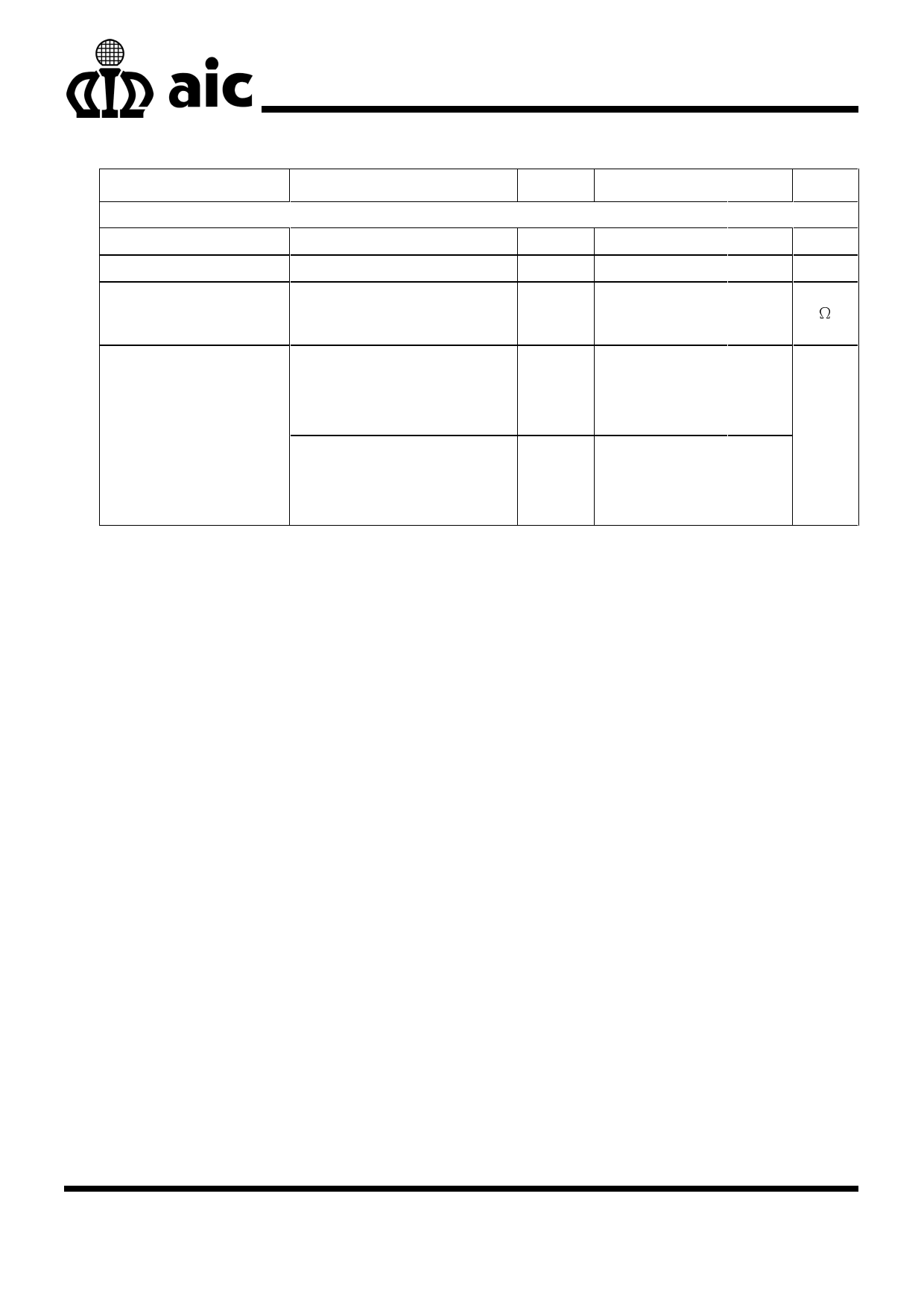
ELECTRICAL CHARACTERISTICS (Continued)
PARAMETER
TEST CONDITIONS
SYMBOL MIN. TYP. MAX. UNIT
Shutdown Pin Specifications
Shutdown Pin Current
VEN = VIN or GND
IEN
0
100
nA
Shutdown Exit Delay Time
IOUT = 30mA
∆t
100
µS
Max Output Discharge
Resistance to GND during
Shutdown
RDSON_
CLMP
20
100
Ω
Chip Enable Low, Output OFF,
VIN = 2.3V to 6.0V
Chip Enable High, Output ON,
VENH
1.6
VIN = 2.3V to 6.0V
Shutdown Input Threshold
Chip Enable Low, Output ON,
VIN = 2.3V to 6.0V
Chip Enable High, Output OFF,
VENL
VIN = 2.3V to 6.0V
V
0.4
Note 1: Specifications are production tested at T =25°C. Specifications over the -40°C to 85°C operating
temperature range are assured by designA, characterization and correlation with Statistical Quality
Controls (SQC).
Note 2: Connecting a 22nF bypass capacitor to BP pin can improve AIC1190 PSRR in High frequency.
7
Share Link: 