AIC1384PSTR 查看數據表(PDF) - Analog Intergrations
零件编号
产品描述 (功能)
比赛名单
AIC1384PSTR Datasheet PDF : 15 Pages
| |||
AIC1384
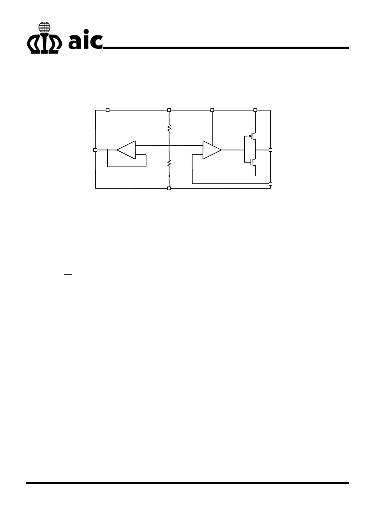
BLOCK DIAGRAM
SD
+
VREF
-
VDDQ
AVIN
50k
-
+
50k
GND
PVIN
VTT
VSENSE
PIN DESCRIPTION
Pin 1: GND - Ground.
Pin 2: SD - Active low shutdown pin.
Pin 3: VSENSE - Sense VTT to improve load
regulation.
Pin 4: VREF
- Buffered output of internal
reference voltage, equal to
VDDQ/2.
Pin 5: VDDQ - Input voltage to internal
reference voltage for regulating
VTT.
Pin 6: AVIN - Analog input voltage to supply
internal control circuitry.
Pin 7: PVIN
- Power input voltage to supply
the rail voltage exclusively for
the output stage used to create
VTT.
Pin 8: VTT
- Regulated output, equal to
VDDQ/2.
Heat Sink - Recommended to Connect to
GND.
9
Share Link: 