AIC1566 查看數據表(PDF) - Analog Intergrations
零件编号
产品描述 (功能)
比赛名单
AIC1566 Datasheet PDF : 7 Pages
| |||
AIC1566
PIN DESCRIPTION
PIN 1: OCSET - Current limit sense pin. Connect
a resistor ROCSET from this pin to
the drain of the external
MOSFET. ROCSET, an internal
200µA current source (IOCSET),
and the external MOSFET on-
resistance (RDS(ON)) jointly set
the over current trip point
according to the following
equation:
IPEAK
=
IOCSET × ROCSET
RDS(ON)
If FB pin voltage is sensed to
be below 50% of the internal
voltage reference VDAC, the
over current comparator
cycles the soft-start function.
PIN 2: SS
PIN 3: VID0
PIN 4: VID1
PIN 5: VID2
PIN 6: VID3
- Soft start pin. Connect a
capacitor from this pin to ground.
An internal 10µA current source
provides soft start function for
the converter.
- 4-bit DAC voltage select pin. TTL
inputs used to set the internal
voltage reference VDAC. When
left open, these pins are
internally pulled up to 5V and
provide logic ones. The level of
VDAC sets the converter output
voltage as well as the PGOOD
and OVP thresholds.
Table 1 specifies the VDAC
voltage for the 16 combinations
of DAC inputs.
PIN 7: COMP - External compensation pin. This
pin is connected to error
amplifier output and PWM
comparator. An RC network is
connected to FB pin to
compensate the voltage-control
feedback loop of the converter.
PIN 8: FB
- The error amplifier inverting
input pin. The FB pin and
COMP pin are used to
compensate the voltage-control
feedback loop.
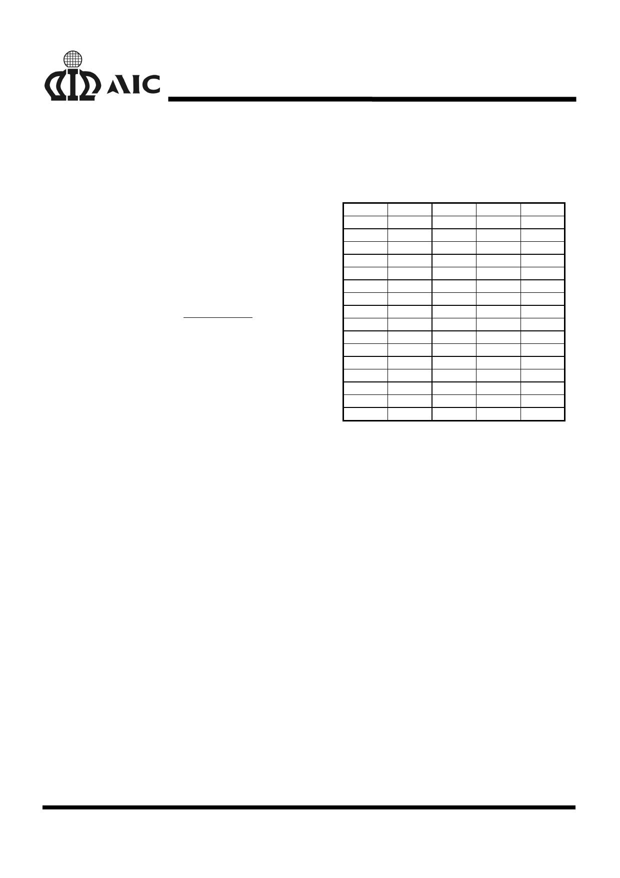
Table 1. Output Voltage Program
VID3
0
0
0
0
0
0
0
0
1
1
1
1
1
1
1
1
VID2
0
0
0
0
1
1
1
1
0
0
0
0
1
1
1
1
VID1
0
0
1
1
0
0
1
1
0
0
1
1
0
0
1
1
VID0
0
1
0
1
0
1
0
1
0
1
0
1
0
1
0
1
VDAC
3.5V
3.4V
3.3V
3.2V
3.1V
3.0V
2.9V
2.8V
2.7V
2.6V
2.5V
2.4V
2.3V
2.2V
2.1V
2.0V
PIN 9: CLP
- Linear regulator current sense
pin. This pin is the positive input
of the current sense
comparator.
PIN 10: CLN
- Linear regulator current sense
pin. This pin is the negative
input of the current sense
comparator.
PIN 11: VLFB - Negative feedback pin for the
linear regulator error amplifier.
PIN 12: LIDRI
- Linear regulator output drive pin.
This pin can drive either a
Darlington NPN or an N-
channel MOSFET.
PIN 13: GND - Signal GND. It also serves as
the power GND for the upper
gate driver.
PIN 14: PGOOD-Power good indicator pin.
PGOOD is an open drain output.
This pin is pulled low when the
converter output is 10% out of
the VDAC reference voltage.
PIN 15: PHASE - Over current detection pin.
Connect the PHASE pin to
source of the external
MOSFET. This pin detects the
voltage drop across the
MOSFET RDS(ON) for over-
6
Share Link: 