AIC1568 查看數據表(PDF) - Analog Intergrations
零件编号
产品描述 (功能)
比赛名单
AIC1568 Datasheet PDF : 7 Pages
| |||
AIC1568
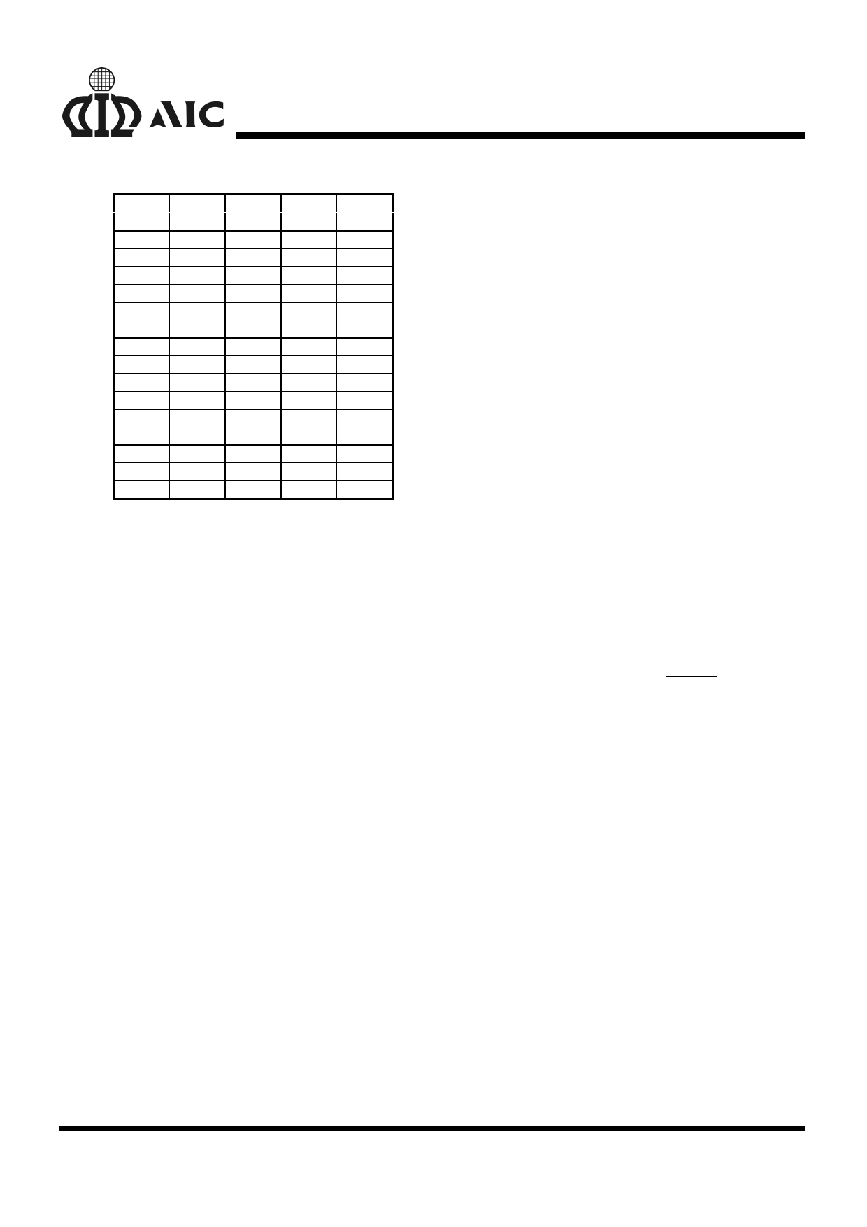
Table 1. Output Voltage Program
VID0 VID1 VID2 VID3 VDAC
0
0
0
0
3.5V
1
0
0
0
3.4V
0
1
0
0
3.3V
1
1
0
0
3.2V
0
0
1
0
3.1V
1
0
1
0
3.0V
0
1
1
0
2.9V
1
1
1
0
2.8V
0
0
0
1
2.7V
1
0
0
1
2.6V
0
1
0
1
2.5V
1
1
0
1
2.4V
0
0
1
1
2.3V
1
0
1
1
2.2V
0
1
1
1
2.1V
1
1
1
1
2.0V
PIN 7: COMP - External compensation pin. This
pin is connected to error
amplifier output and PWM
comparator. An RC network is
connected to FB pin to
compensate the voltage-control
feedback loop of the converter.
PIN 8: FB
- The error amplifier inverting
input pin. The FB pin and COMP
pin are used to compensate the
voltage-control feedback loop.
PIN 9: GND
- Signal GND. It also serves as
the power GND for the upper
gate driver.
PIN 10: PGOOD-Power good indicator pin.
PGOOD is an open drain output.
This pin is pulled low when the
converter output is ±10% out of
the VDAC reference voltage.
PIN 11: PHASE - Over current detection pin. Connect
the PHASE pin to source of the
external MOSFET. This pin detects
the voltage drop across the MOSFET
RDS(ON) for over-current protection.
PIN 12: UGATE- External MOSFET gate drive pin.
Connect this pin to gate of the
external MOSFET.
PIN 13: BOOT - External MOSFET driver power
supply pin. To convert 5V main power
to VCORE power by driving N-channel
MOSFET, supply voltage of no
higher than 12V is recommended
since the negative power terminal of
the internal driver is internally tied to
GND.
PIN 14: VCC - The chip power supply pin.
Recommended supply voltage is 12V.
PIN 15: RT/OVP- Frequency
adjustment
and
overvoltage indicator pin. This pin is
multiplexed to provide two functions.
The first function is oscillator
switching frequency adjustment.
Connecting a resistor (RT) from this
pin to GND increases the frequency
according to the following equation:
FS
≅
2 0 0KHz
+
5 × 10⁵
lo g RT
The second function for this pin is to
drive an external SCR in the event of
an over voltage fault.
PIN 16: VSEN - Converter output voltage sense pin.
Connect this pin to the converter
output. The PGOOD and OVP
comparator circuits use this signal to
report output voltage status and
perform overvoltage protection
function.
6
Share Link: 