AIC1731 查看數據表(PDF) - Analog Intergrations
零件编号
产品描述 (功能)
比赛名单
AIC1731 Datasheet PDF : 10 Pages
| |||
AIC1731
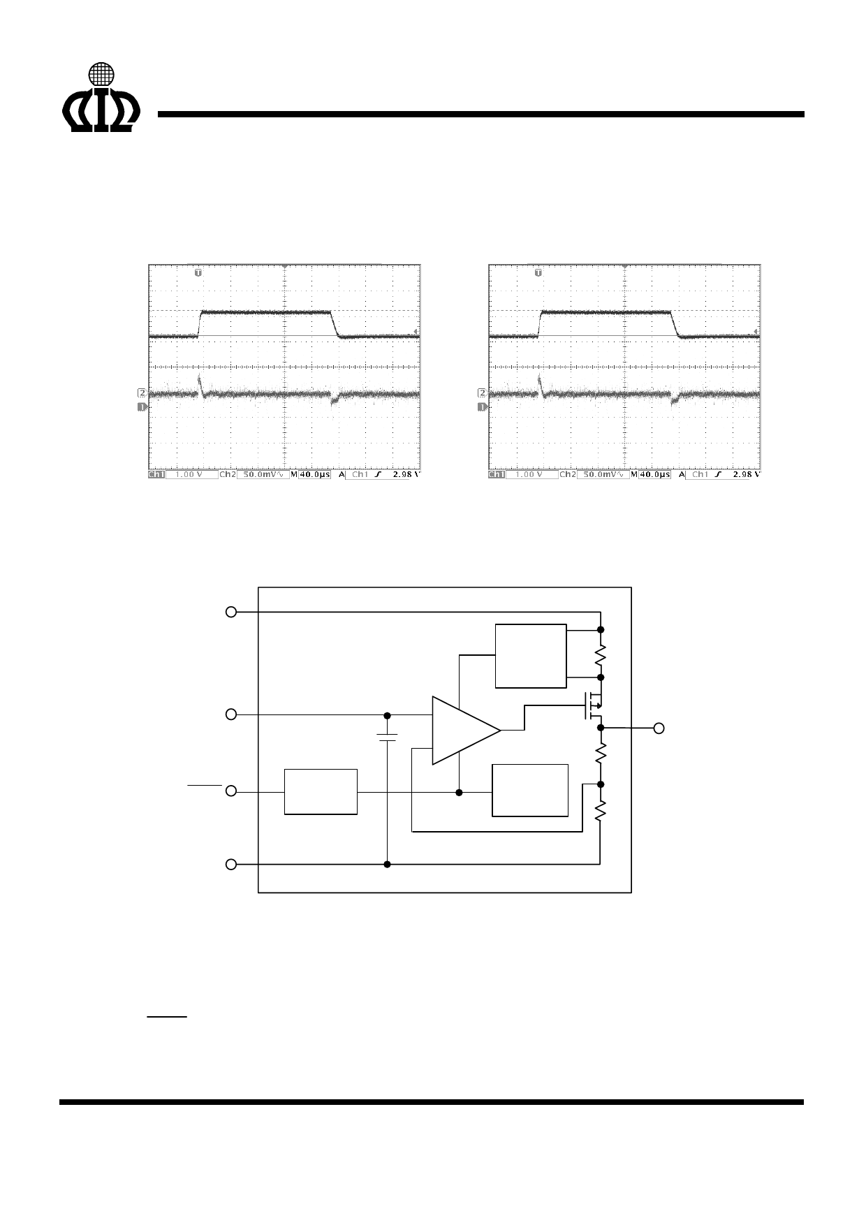
TYPICAL PERFORMANCE CHARACTERISTICS (Continued)
VIN=Vout+2V
Vin=Vout+1V
VIN=Vout+2V
VIN=Vout+1V
VOUT=1.5V
CIN=1µF, COUT=1µF
CBP=0.1µF
Iout=50mA
Fig. 17 Line Transient Response
VOUT=1.5V
CIN=1µF, COUT=4.7µF
CBP=0.1µF
Iout=50mA
Fig. 18 Line Transient Response
BLOCK DIAGRAM
VIN
Current
Limiting
BP
SHDN
VREF
1.23V
Power
Shutdown
- Error
Amp.
+
Thermal
Limiting
VOUT
GND
PIN DESCRIPTIONS
PIN 1 : VIN - Power supply input pin. Bypass
with a 1µF capacitor to GND
PIN 2 : GND - Ground pin.
PIN 3 : SHDN - Active-Low shutdown input pin.
PIN 4 : BP - Noise bypass pin. An external
bypass capacitor connected to
BP pin reduces noises at the
output.
PIN 5 : VOUT - Output pin. Sources up to 300
mA.
8
Share Link: 