AOZ1083 查看數據表(PDF) - Alpha and Omega Semiconductor
零件编号
产品描述 (功能)
比赛名单
AOZ1083 Datasheet PDF : 12 Pages
| |||
AOZ1083
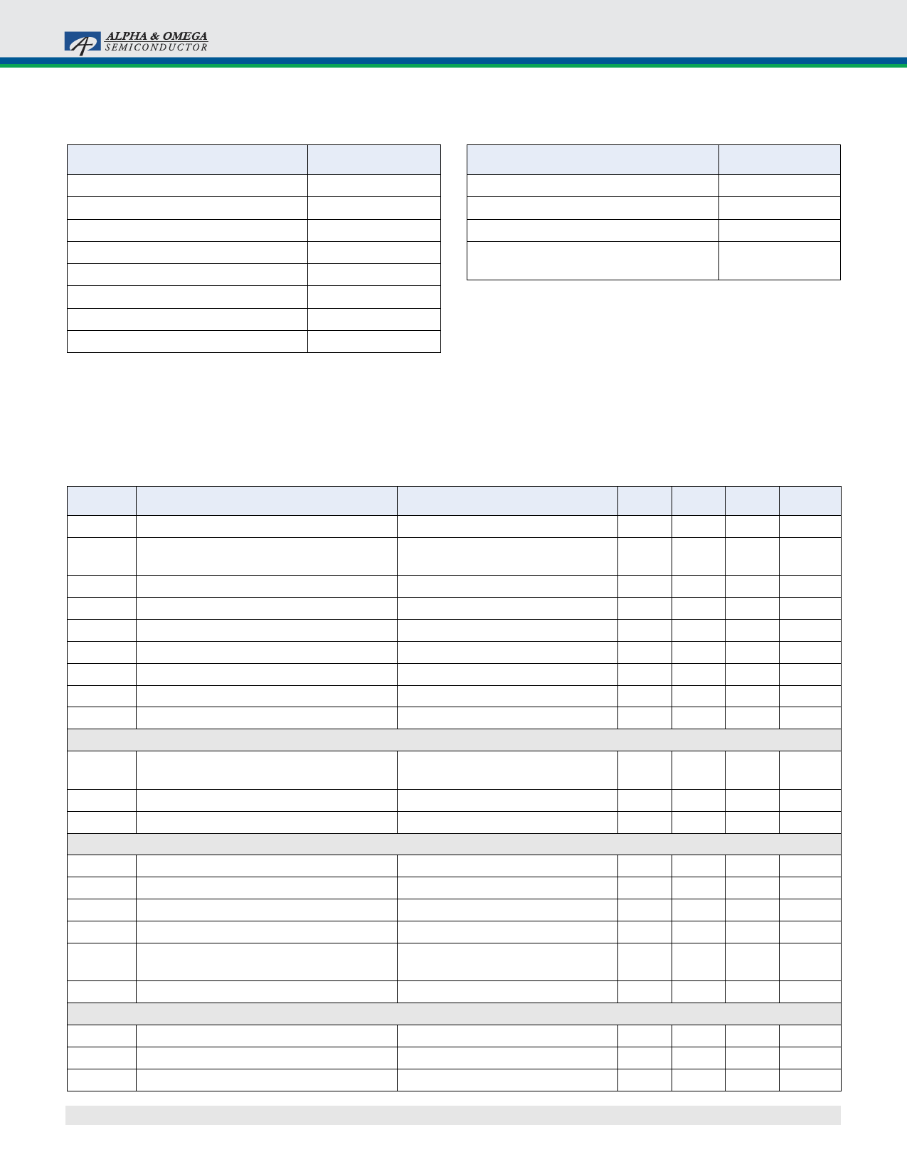
Absolute Maximum Ratings
Exceeding the Absolute Maximum Ratings may damage the
device.
Parameter
Rating
Supply Voltage (VVIN)
LX to GND
DIM to GND
FB to GND
BST to AGND
Junction Temperature (TJ)
Storage Temperature (TS)
ESD Rating(1)
30 V
-0.7 V to VVIN+ 2 V
-0.3 V to 26 V
-0.3 V to 6 V
VLX + 6 V
+150 °C
-65 °C to +150 °C
2 kV
Note:
1. Devices are inherently ESD sensitive, handling precautions are
required. Human body model rating: 1.5 kΩ in series with 100 pF.
Recommended Operating Conditions
The device is not guaranteed to operate beyond the
Recommended Operating Conditions.
Parameter
Rating
Supply Voltage (VVIN)
Output Voltage Range
Ambient Temperature (TA)
Package Thermal Resistance (ΘJA)
SOT23-6L(2)
3.0 V to 26 V
Up to 0.85 x VVIN
-40 °C to +85 °C
220 °C/W
Note:
2. The value of ΘJA is measured with the device mounted on a 1-in2
FR-4 board with 2 oz. Copper, in a still air environment with
TA = 25 °C. The value in any given application depends on the
user’s specific board design.
Electrical Characteristics
TA = 25 °C, VVIN = VDIM = 12 V. Specifications in BOLD indicate a temperature range of -40 °C to +85 °C. These specifications are
guaranteed by design.
Symbol
Parameter
Conditions
Min. Typ. Max. Units
VVIN
VUVLO
Supply Voltage
Input Under-Voltage Lockout Threshold
UVLO Hysteresis
IVIN Supply Current (Quiescent)
IOFF Shutdown Supply Current
VFB Feedback Voltage
VFB_LOAD Load Regulation
VFB_LINE Line Regulation
IFB Feedback Voltage Input Current
PWM DIMMING
VDim_OFF Dimming Input Threshold
VDim_ON
VDim_HYS Dimming Input Hysteresis
IDIM Dimming Input Current
MODULATOR
fO
DMAX
TON_MIN
ILIM
Frequency
Maximum Duty Cycle
Minimum On Time
Current Limit
Over-Temperature Shutdown Limit
TSS Soft Start Interval
POWER STATE OUTPUT
RDS(ON)
RDS(ON)
ILEAKAGE
NMOS On-Resistance
NMOS On-Resistance
NMOS Leakage
VVIN Rising
VVIN Falling
IOUT = 0, VFB = 1 V, VDIM > 1.2 V
VDIM = 0 V
TA = 25 ºC
120 mA < Load < 1.08 A
Load = 600 mA
VFB = 280 mV
Off Threshold
On Threshold
TJ Rising
TJ Falling
VIN = 12 V
VIN = 3.3 V
VDIM = 0 V, VLX = 0 V
3
26
V
2.9
V
2.3
V
200
mV
1
1.5
mA
8
μA
266 280 294
mV
0.5
%
0.03
%/V
500
nA
0.4
V
1.2
V
200
mV
3
μA
1.2
1.5
1.8
MHz
87
%
100
ns
1.5
1.9
2.3
A
150
°C
110
°C
400
μs
240
mΩ
380
mΩ
10
μA
Rev. 1.0 July 2011
www.aosmd.com
Page 3 of 12
Share Link: 