APL78L05 查看數據表(PDF) - Anpec Electronics
零件编号
产品描述 (功能)
比赛名单
APL78L05 Datasheet PDF : 17 Pages
| |||
APL78L05/12
Pin Description
SOP-8
1
2,3,6,7
4,5
PIN
NO.
TO-92 SOT-89
1
1
2
2
-
-
NAME
VOUT
GND
NC
8
3
3
VIN
FUNCTION
Output Voltage Output Pin.
Ground. A common ground is required between the input and the output voltage.
No Internal Connection
Power input pin of the device. The maximum Input Voltage can be 30V. It should be
bypassed with a 0.33µF (minimum) capacitor to the GND.
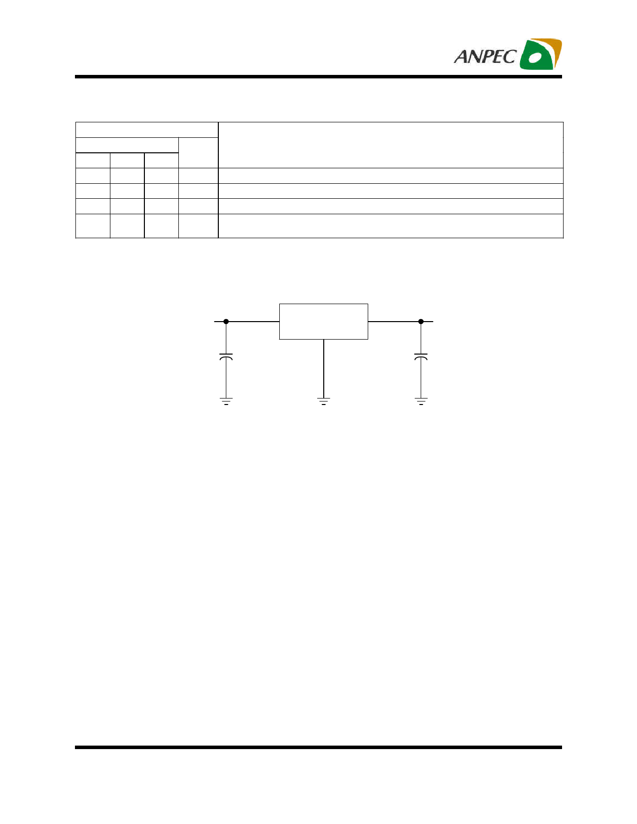
Typical Application Circuit
VIN
CIN=
0.33µF
APL78L05/12
VOUT
COUT=
0.1µF
Note
a : A common ground is required between the input and the output voltage. The input voltage must remain typically 2V above the
output voltage even during the low point on the input ripple voltage.
b : CIN is required if regulator is located an appreciable distance from power supply filter.
c : COUT is not needed for stability; however, it improves transient response.
Copyright © ANPEC Electronics Corp.
7
Rev. A.11 - Jun., 2011
www.anpec.com.tw
Share Link: 