APX9266 查看數據表(PDF) - Anpec Electronics
零件编号
产品描述 (功能)
比赛名单
APX9266 Datasheet PDF : 14 Pages
| |||
APX9266
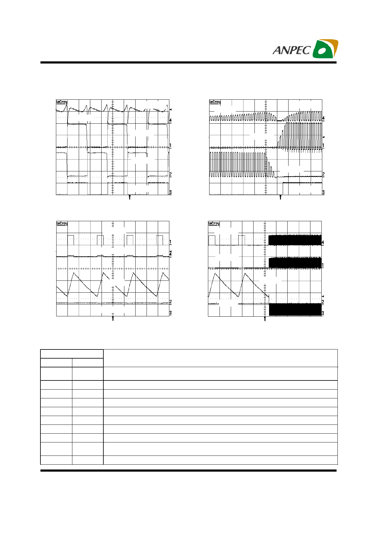
Operating Waveforms (Cont.)
Rotation Waveform 3
Full Speed
IIN (200mA/div)
OUT2(2V/div)
Rotation Waveform 4
IIN (200mA/div)
PWM Mode
OUT2(2V/div)
OUT1(2V/div)
FG(5V/div)
Time (0.2ms/div)
Lock Protection Waveform 1
OUT1(5V/div)
OUT2(5V/div)
OUT1(2V/div)
Time (0.2ms/div)
FG(5V/div)
Lock Protection Waveform 2
OUT1(5V/div)
OUT2(5V/div)
CT(0.5V/div)
CT(0.5V/div)
FG(5V/div),always High
Time (1s/div)
FG(5V/div)
Time (1s/div)
Pin Description
PIN
No.
Name
1
OUT2
2
CT
3
IN+
4
HB
5
IN-
6
FG
7
PWM
8
VCC
9
OUT1
10
GND
Description
H-bridge Output Connection. The output stage is a H-bridge formed by four transistors and
four-protection diode for switching applications.
Shutdown Time and Restart Time Setting.
Hall Input +.
Hall Bias.
Hall Input -.
Rotation Speed Output.
PWM Signal Input Terminal.
Supply Voltage Input Pin.
H-bridge Output Connection. The output stage is a H-bridge formed by four transistors and
four-protection diode for switching applications.
Power Ground.
Copyright © ANPEC Electronics Corp.
6
Rev. A.4 - Mar., 2008
www.anpec.com.tw
Share Link: 