AS1329 查看數據表(PDF) - austriamicrosystems AG
零件编号
产品描述 (功能)
比赛名单
AS1329 Datasheet PDF : 17 Pages
| |||
AS1329
Data Sheet - Application Information
PCB Layout Guidelines
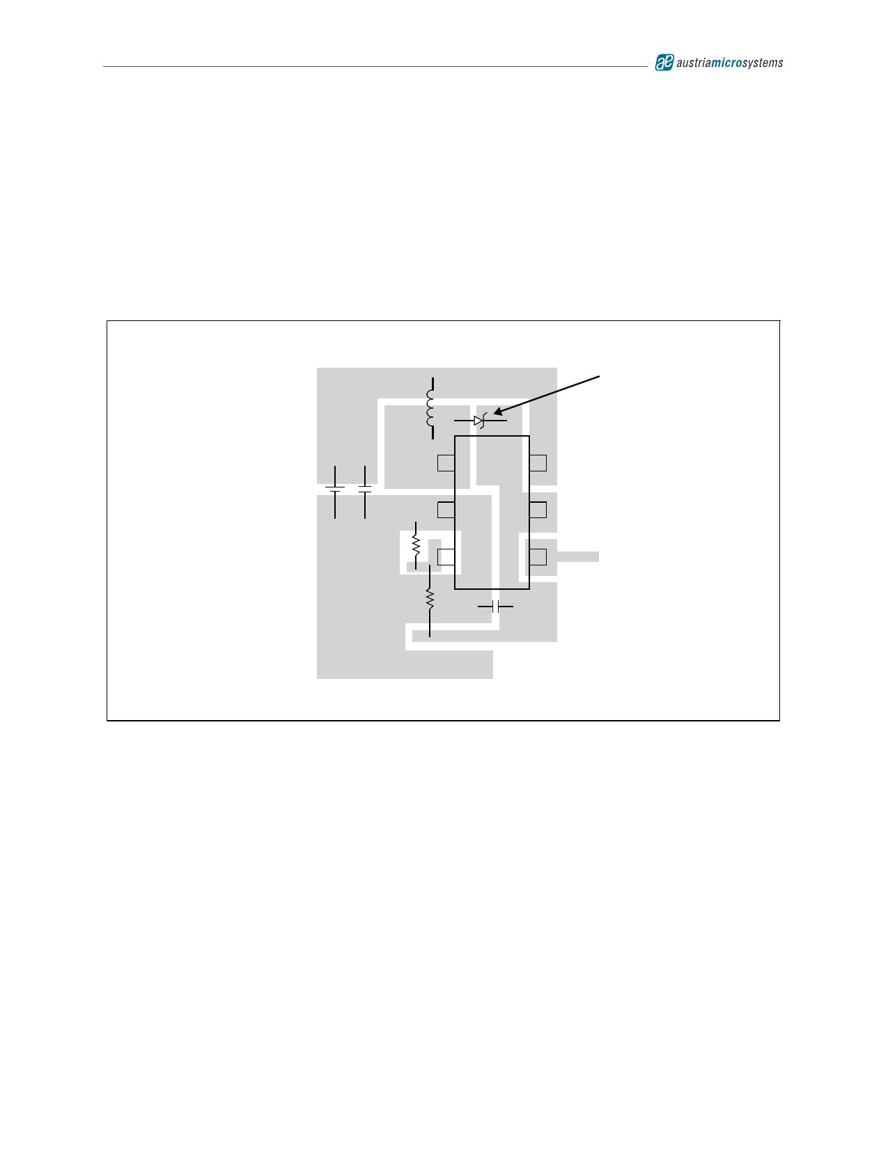
The high-speed operation of the AS1329 requires proper layout for optimum performance. Figure 21 shows the recom-
mended component layout.
! A large ground pin copper area will help to lower the device temperature.
! A multi-layer board with a separate ground plane is recommended.
! Traces carrying large currents should be direct.
! Trace area at pin FB should be as small as is practical.
! The lead-length to the battery should be as short as is practical.
Figure 21. Recommended Single-Layer Component Placement
Optional
1 SW
VIN 6
AS1329
VIN
R2 2 GND VOUT 5
CIN
3 FB SHDNN 4
SHDNN
R1
COUT
VOUT
www.austriamicrosystems.com
Revision 1.01
13 - 17
Share Link: 