AS6C6264-55STIN 查看數據表(PDF) - Alliance Semiconductor
零件编号
产品描述 (功能)
比赛名单
AS6C6264-55STIN Datasheet PDF : 12 Pages
| |||
February 2007
®
8K X 8 BIT LOW POWER CMOS SRAM
AS6C6264
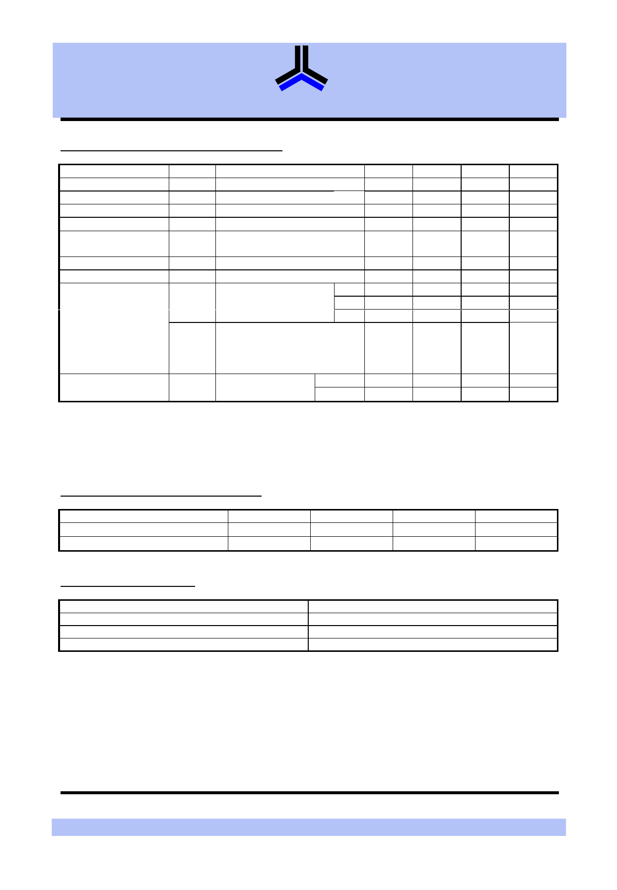
DC ELECTRICAL CHARACTERISTICS
PARAMETER SYMBOL
TEST CONDITION
Supply Voltage
Input High Voltage
Input Low Voltage
Input Leakage Current
Output Leakage
Current
VCC
VIH*1
VIL*2
ILI
ILO
VCC >= VIN >= VSS
VCC >= VOUT >= VSS,
Output Disabled
Output High Voltage
VOH IOH = -1mA
Output Low Voltage
VOL IOL = 2mA
Cycle time = Min.
Average Operating
Power supply Current
ICC CE# = VIL and CE2 = VIH, - 55
II/O = 0mA
Cycle time = 1µs
ICC1
CE#≦0.2V and CE2≧VCC-0.2V,
II/O = 0mA
Standby Power
Supply Current
other pins at 0.2V or VCC-0.2V
ISB1
CE# >= VCC-0.2V
or CE2≦0.2V
-C
-I
Notes: C = Commercial Temperature I = Industrial temperature
1. V IH(max) =VCC + 3.0V for pulse width less than 10ns.
2. V IL(min) =VSS - 3.0V for pulse width less than 10ns.
3. Over/Undershoot specifications are characterized, not 100% tested.
4. 10 µA for special request
5. Typical values are included for reference only and are not guaranteed or tested.
Typical valued are measured at VCC = VCC(TYP.) and TA = 25ºC
MIN.
2.7
2.4V
- 0.5
-1
-1
2.4
-
-
-
-
TYP. *5
3.0
-
-
-
MAX.
5.5
VCC+0.3
0.6
1
-
1
3.0
-
-
0.4
UNIT
V
V
V
µA
µA
V
V
15
45
mA
3
10
mA
1
50*4
µA
1
80*4
µA
CAPACITANCE (TA = 25ºC, f = 1.0MHz)
PARAMETER
SYMBOL
MIN.
Input Capacitance
CIN
-
Input/Output Capacitance
CI/O
-
Note :These parameters are guaranteed by device characterization, but not production tested.
MAX
6
8
UNIT
pF
pF
AC TEST CONDITIONS
Input Pulse Levels
Input Rise and Fall Times
Input and Output Timing Reference Levels
Output Load
0.2V to VCC - 0.2V
3ns
1.5V
CL = 50pF + 1TTL, IOH/IOL = -1mA/2mA
02/Feb/07, v1.0
Alliance Memory Inc
Page 3 of 12
Share Link: 