LA4276 查看數據表(PDF) - SANYO -> Panasonic
零件编号
产品描述 (功能)
比赛名单
LA4276 Datasheet PDF : 6 Pages
| |||
LA4276
Description of External Parts
C1, C5: Feedback capacitors
Decreasing the capacitance value lowers the low frequency response. Increasing the capacitance value makes the
starting time later.
C2, C4: Input capacitors
C3: Ripple filter capacitor
Decreasing the capacitance value too far or eliminating it altogether causes ripple to occur. However, ripple is not
necessarily reduced if the capacitance value is increased. This capacitor also affects the starting time; decreasing the
capacitance value makes the starting time earlier.
C6, C9: Output capacitors
Decreasing the capacitance value causes insufficient power at low frequencies.
C7, C10: Oscillation blocking capacitors
Decreasing the capacitance value causes oscillation to occur easily. Use a mylar film capacitor that has good high
frequency response and temperature characteristics. The use of an electrolytic capacitor or a ceramic capacitor may
cause oscillation to occur at low temperatures.
C8: Power capacitor
Decreasing the capacitance value causes ripple to occur easily. Locating this capacitor at a distance from the IC or
removing this capacitor may cause oscillation to occur.
R1, R5: Feedback resistors
Refer to supplementary discussion “Voltage Gain.”
R2, R4: Input bias resistors
These determine the bias (GND potential bias) and the input impedance of the input pins. If a variable resistor or
other device also serves this function, these resistors can be omitted.
R3: Muting resistor
Refer to supplementary discussion “External Muting.”
R6, R7: Resistors connected in series with oscillation blocking capacitor
These prevent phase shift in conjunction with the oscillation blocking capacitor so that oscillation does not easily
occur. There is an optimal value for the resistor; increasing or decreasing the resistance causes oscillation to occur
easily.
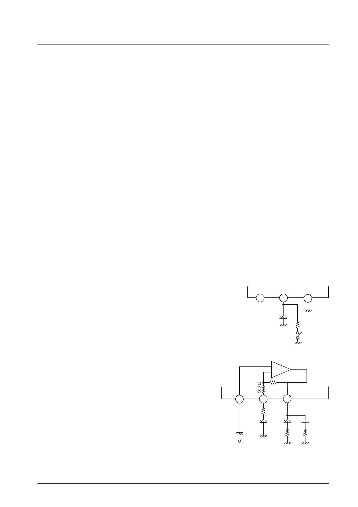
External Muting
• Pull down the electric potential of the ripple filter pin (pin 3).
Muting becomes possible by inserting the discharge resistor R3 between pin 3
and GND. If the resistance value of R3 is too low, a popping noise is generated; if
the resistance value is too high, the muting effect is reduced. (A value of 200 Ω is
recommended for R3.)
IN1
2
Filter
3
PRE GND
4
+
C3
R3
Mute SW
Voltage Gain
The voltage gain can be lowered by adding external resistors R1/R5 in
series to feedback capacitors C1/C5. When R1/R5 = 150 Ω, the voltage
gain is 40 dB. However, it is important to note that because there is no
phase compensation pin, decreasing the voltage gain can extend the high
frequency characteristics, allowing oscillation to occur easily.
RNF
Rf 30 kΩ
IN1/2
5
(2)
NF1/2
6
(1)
OUT1/2
7
(10)
R1/R5
+
+
C2/C4
C1/C5
+
C6/C9
RL
C7/C10
R2/R3
No. 7094-3/6
Share Link: 