AV3843B 查看數據表(PDF) - Avic Technology
零件编号
产品描述 (功能)
比赛名单
AV3843B Datasheet PDF : 6 Pages
| |||
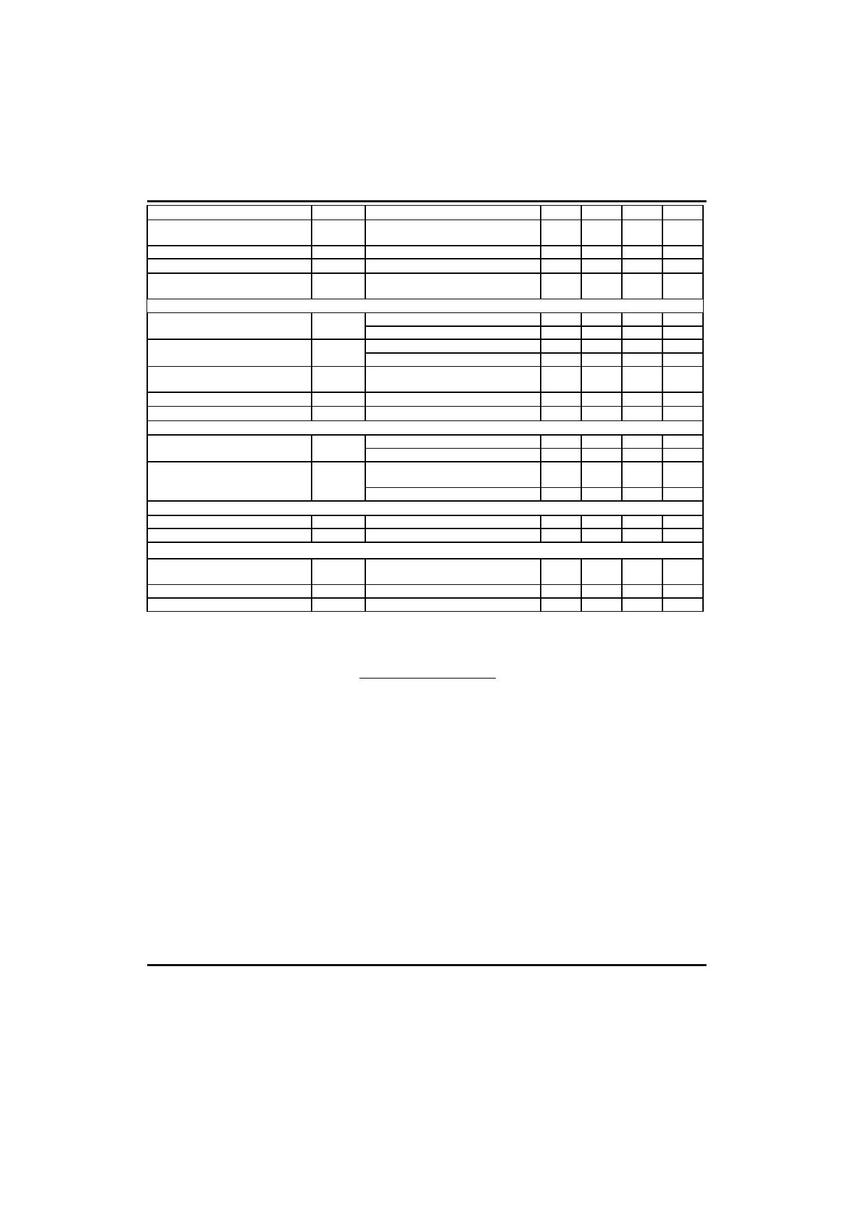
@vic AV3842B / 3843B LINEAR INTEGRATED CIRCUIT
PARAMETER
Maximum Current Sense Input
Threshold
Power Supply Rejection Ratio
Input Bias Current
SYMBOL
Vth
PSRR
IIB
TEST CONDITIONS
(note 3)
12<=Vcc<=25V (note 3)
Propagation Delay
Output Section
Output Low Voltage
tPLH(In/O
ut)
VOL
Output High Level
VOH
Output Voltage with UVLO
VOL
Activated
(UVLO)
Output Voltage Rise Time
tr
Output Voltage Fall Time
tf
Under-Voltage Lockout Section
Startup Threshold
Vth
Min. Operating Voltage After
Turn-on(Vcc)
VCC(min)
PWM Section
Current Sense Input to Output
Isink=20mA
Isink=200mA
Isource=20mA
Isource=200mA
Vcc=6.0V,Isink=1.0mA
Tj=25°C,CL=1nF
Tj=25°C,CL=1nF
UTC UC3842B
UTC UC3843B
UTC3842B
UTC3843B
Maximum Duty Cycle
Minimum Duty Cycle
Total Device
DC(MAX)
DC(MIN)
Power Startup Supply Current
Power Operating Supply Current
Power Supply Zener Voltage
Icc+Ic
Icc+Ic
Vz
Vcc=6.5V for UC3843B
Vcc=14V for UC3842B
Note2
Icc=25mA
Note 1:Maximum Package power dissipation limits must be observed.
Note 2:Adject Vcc above the Startup threshold before setting to 15V.
Note 3:This parameter is measured at the latch trip point with VFB=0V.
Note 4:Comparator gain is defined as :
∆V Output Compensation
AV
∆V Current Sense Input
MIN TYP MAX UNIT
0.9 1.0 1.1
V
70
dB
-2
-10
µA
150 300 ns
0.1 0.4
V
1.6 2.2
V
13 13.5
V
12 13.4
V
0.1 1.1
V
50 150 ns
50 150 ns
14.5 16 17.5 V
7.8 8.4
9
V
8.5
10 11.5
V
7.0 7.6 8.2
V
94
96
%
0
%
0.3 0.5 mA
12
17
mA
30
36
V
QW-R103-012,A
Share Link: 