MM1188 查看數據表(PDF) - Mitsumi
零件编号
产品描述 (功能)
比赛名单
MM1188 Datasheet PDF : 5 Pages
| |||
MITSUMI
3-Input 1-Output Video Switch (with Y-C mix) MM1188
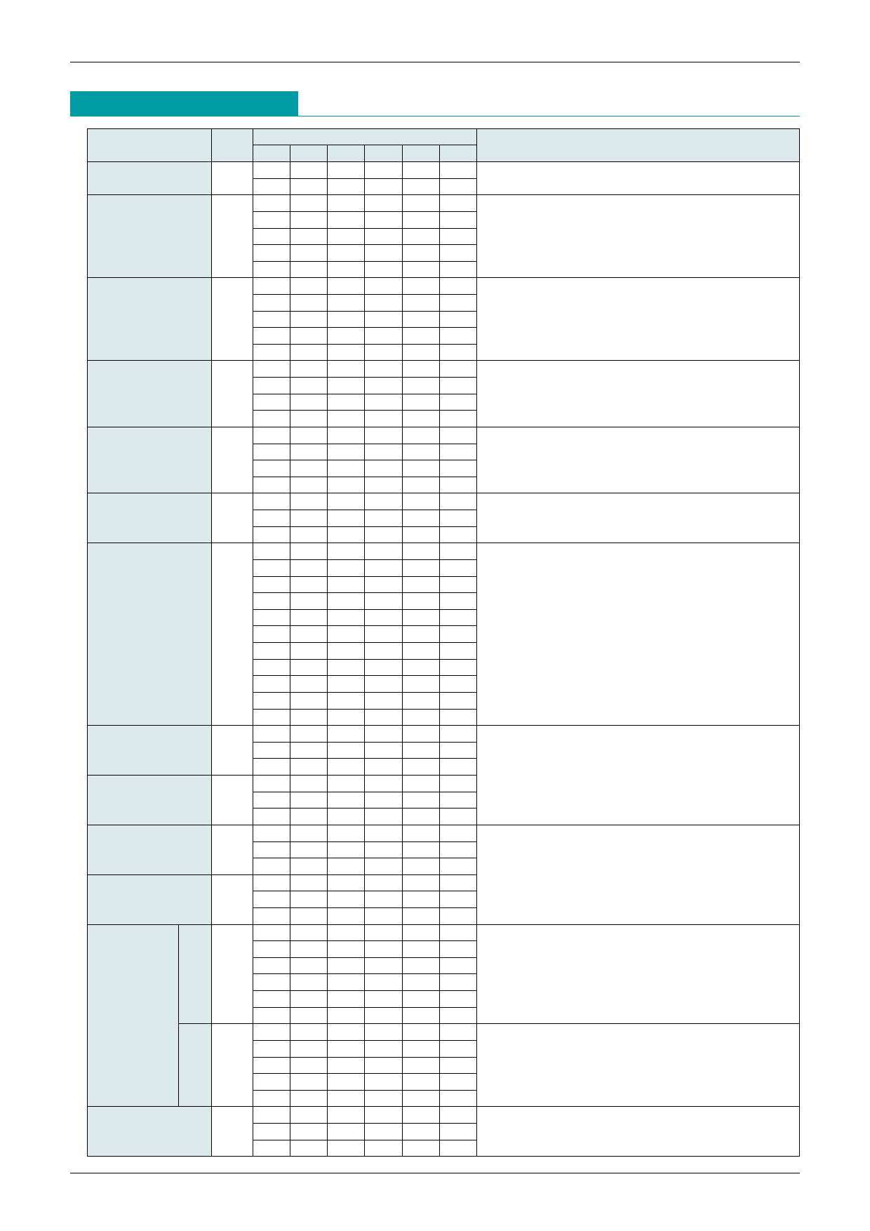
Measuring Procedures (Except where noted otherwise, VCC=12.0V, VC1=VCC, VC2=0V)
Item
Symbol S1
Switch state
S2 S3 S4 S5
S6
Measuring Procedure
Consumption
current
Id
2
2
2
2
2
2 Connect a DC ammeter to the VCC pin and measure. The
ammeter is shorted for use in subsequent measurements.
1 2 2 2 2 2 Input a 1.0VP-P, 100kHz sine wave to SG, and
2 1 2 2 2 2 obtain Gv from the following formula given TP1
Voltage gain GV 2 2 1 2 1 2 voltage as V1 and TP3 voltage as V2.
222111
222121
GV=20LOG (V2/V1) dB
1 2 2 2 2 2 For the above GV measurement, given TP3
Frequency
characteristic
FC
2
2
2
1
2
2
2
1
2
2
2
1
2
1
1
2 voltage for 10MHz as V3, FC is obtained from the
2 following formula.
1
222121
FC=20LOG (V3/V2) dB
2 1 2 2 2 2 Input a 1.0VP-P staircase wave to SG, and
Differential gain DG
2
2
2
2
1
2
2
1
1
1
* 2 measure differential gain at TP3. 1
1
222121
APL=10~90%
212222
Differential phase DP
2
2
2
2
2
2
1
2
2
2
1
1
1
1
2
2 Proceed as for DG, and measure differential
* 1 phase. 2
1
Output offset
voltage
2
Voff 2
2
2
2
2
2
2
2
2
2
2
2
1
1
2
2
1
Measure the DC voltage difference of each
switch status at TP2.
122212
122221
1 2 2 2 1 1 Assume VC1=2.3V, VC2=0.9V.
2 1 2 2 1 2 Input a 1.0VP-P, 4.43MHz sine wave to SG, and
2 1 2 2 2 1 given TP3 voltage during signal output as V4,
Crosstalk
CT 2 1 2 2 1 1 switch S5 and S6, and given TP3 voltage for
2 2 1 2 2 2 output OFF as V5, CT is obtained from the
2 2 1 2 2 1 following formula.
221211
222122
CT=20LOG (V5/V4) dB
222112
Switch 1 input
voltage H
VIH1
2
2
2
2
1
2 Impress an optional DC voltage on TP7 and TP8.
Gradually raise from VC1=0V. TP4 voltage when
TP8 voltage is output on TP2 is VIH1. Gradually
Switch 1 input
voltage L
VIL1
lower from VC1=VCC. TP4 voltage when TP7
voltage is output on TP2 is VIL1.
Switch 2 input
voltage H
VIH2
2
2
2
2
2
1 Impress an optional DC voltage on TP7 and TP9.
Gradually raise from VC1=0V. TP5 voltage when
TP9 voltage is output on TP2 is VIH2. Gradually
Switch 2 input
voltage L
VIL2
lower from VC1=VCC. TP5 voltage when TP7
voltage is output on TP2 is VIL2.
3 1 2 2 2 2 Input a luminance signal as shown in Figure 1 to
SG1, and a chroma signal as shown in Figure 2
A DRA
to SG2. Change the chroma signal amplitude and
measure the maximum amplitude where there is
IN1-C input
no waveform distortion at TP3 and convert to
dynamic
input amplitude.
range
3 1 2 2 2 2 Input a luminance signal as shown in Figure 3 to SG1,
and a chroma signal as shown in Figure 2 to SG2.
B DRB
Change the chroma signal amplitude and measure the
maximum amplitude where there is no waveform
distortion at TP3 and convert to input amplitude.
IN1-Y, IN2, IN3
2 1 2 2 2 2 Input a sine wave to SG1. Measure the maximum
input dynamic DRC 2 2 1 2 1 2 amplitude where there is no waveform distortion
range
2 2 2 1 1 1 at TP3 and convert to input amplitude.
Share Link: 