G9611 查看數據表(PDF) - Global Mixed-mode Technology Inc
零件编号
产品描述 (功能)
比赛名单
G9611 Datasheet PDF : 7 Pages
| |||
Global Mixed-mode Technology Inc.
G9611
Absolute Maximum Ratings
Supply Voltage (IN or OUT to GND……..-0.3V to +6.5V
Output Short-Circuit Duration…………….…………1 min
Input Voltage …………………..…-0.3V to the greater of
(IN+0.3V) or (OUT + 0.3V)
Continuous Power Dissipation (TA = +25°C)…...700mW
Operating Temperature Range……..…. -40°C to +85°C
Junction Temperature……………….……………+160°C
Storage Temperature Range…..…..….-65°C to +160°C
Lead Temperature (soldering, 10sec)…...….…..+260°C
Stresses beyond those listed under "Absolute Maximum Ratings" may cause permanent damage to the device. These are stress ratings
only, and functional operation of the device at these or any other conditions beyond those indicated in the operational sections of the
specifications is not implied. Exposure to absolute maximum rating conditions for extended periods may affect device reliability
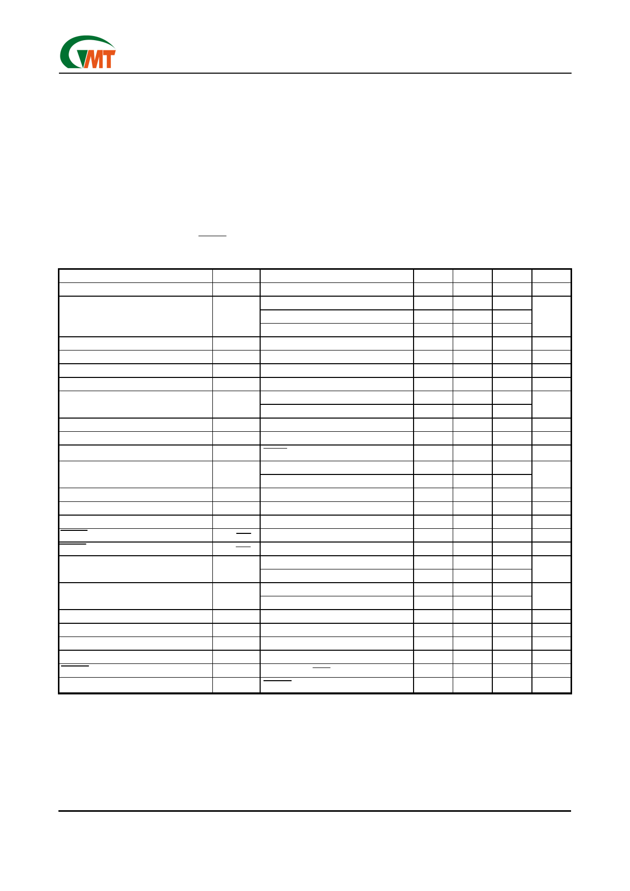
Electrical Characteristics
VIN=5V, CIN=1µF, COUT=10µF, SHDN =VIN, TJ =TA=25°C (Note3), unless otherwise noted. Typical values for
regulators are at VIN =5V.
PARAMETER
Input Voltage
Output Voltage (Note 1)
Load Regulation
Line Regulation
Dropout Voltage (Note 2)
Parameter Tempco VOUT
Ripple Rejection
Output Noise
Quiescent Current
OFF Quiescent Current
Foldback Current Limit
Foldback Voltage
Thermal Shutdown Temperature
Thermal Shutdown Hysteresis
SHDN Pin Input High Threshold
SHDN Pin Input Low Threshold
Reset Threshold
Reset Threshold Hysteresis
Reset Threshold Tempco
CD Delay Pin Threshold Voltage
CD Pin Sink Current
CD Pin Pullup Resistance
RESET Output Current Low
RESET Function Operating Voltage
SYMBOL
CONDITION
VIN
G9611A
VOUT G9611B/C
G9611D
∆VLDR
∆VLNR
∆VDO
IOUT=1mA to 300mA, VIN=VOUT +1V
(VOUT+0.5V) ≤ VIN ≤ 6V, IOUT =25mA
IOUT=300mA
PSRR
en
IQ
IQOFF
f=120HZ, IOUT=30mA
f=120HZ, IOUT=300mA
20Hz to 100kHz, IOUT=30mA.
SHDN ≤0.4V
ILIM
VOUT<VFOLDBACK
VOUT>VFOLDBACK
VFOLDBACK
TSD
∆TSD
VIH_ SHDN
VIL_ SHDN
G9611A/B/D
VTH-
G9611C
VHYS
G9611A/B/D
G9611C
VTCD
ICD
RD
IOL
VOP
VCC = 5V
VCC=1.5V, VCD=0.5V
VCC=2.5V, V RESET =0.4V
RESET sink current>10µA
MIN
2.5
3.332
3.234
2.45
---
-8
---
---
---
---
---
---
---
260
650
0.6
---
---
1.8
0.6
4.11
3.81
---
---
---
3.5
3
100
8
---
TYP
---
3.4
3.3
2.5
6
0.3
320
40
70
65
350
320
140
400
900
0.78
160
30
2
0.8
4.2
3.9
150
130
40
3.9
4.3
200
11.5
0.7
MAX
6.0
3.468
3.366
2.55
15
8
400
---
---
---
---
450
200
580
1200
0.95
---
---
2.3
1.1
4.29
3.99
---
---
---
4.3
---
400
---
0.85
UNIT
V
V
mV
mV
mV
ppm/°C
dB
µVRMS
µA
µA
mA
V
°C
°C
V
V
V
mV
ppm/°C
V
mA
kΩ
mA
V
Note 1: (VIN-VOUT) is limited to keep the product (IOUT x (VIN - VOUT)) from exceeding the package power dissipation
limits.
Note 2: Dropout Voltage is (VIN - VOUT) when VOUT falls to 100mV below its nominal value at VIN = VOUT+1V. For
example, the G9611 is tested by measuring the VOUT at VIN = VOUT+1V, then VIN is lowered until VOUT falls
100mV below the measured value. The difference (VIN - VOUT) is then measured and defined as ∆VDO.
Note 3: Low duty pulse techniques are used during test to maintain junction temperature as close to ambient as possible.
Ver: 1.4
Jun 29, 2004
TEL: 886-3-5788833
http://www.gmt.com.tw
2
Share Link: 