G9611CP1T 查看數據表(PDF) - Global Mixed-mode Technology Inc
零件编号
产品描述 (功能)
比赛名单
G9611CP1T Datasheet PDF : 7 Pages
| |||
Global Mixed-mode Technology Inc.
Pin Description
G9611
PIN NO.
1, 6
2
3
4
5
7
8
PIN NAME
N.C
RESET
SHDN
VIN
VOUT
GND
CD
PIN FUNCTION
No Connection.
RESET Open-Drain Output remains low while VIN is below the reset threshold,
and for delay time set by CD after VIN rises above the reset threshold.
SHDN = High to enable regulator output.
SHDN = Low to shutdown regulator output.
Regulator Input. Supply voltage can range from 2.5V to 6V.
Regulator Output. Sources up to 300mA.
Ground
External Programmable time delay is set by the capacitor connect to CD pin.
-
SHDN
SHUTDOWN
LOGIC
+
THERMAL
PROTECTION
1.24V
REFERENCE
VIN
MOSFET DRIVER
WITH FOLDBACK
CURRENT LIMIT
P
VOUT
-
+
R1
R2
GND
RESET
RD
CD
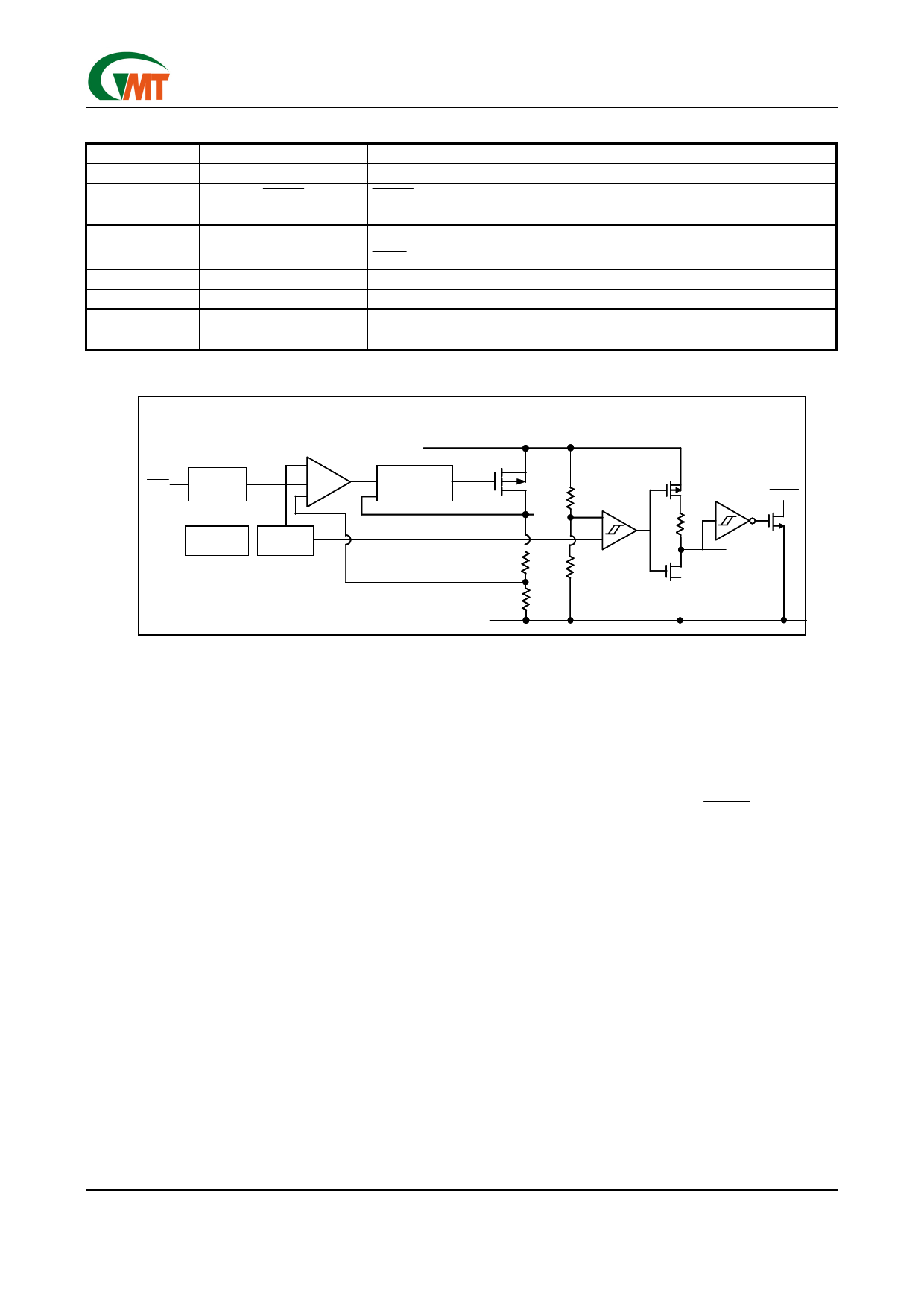
Figure 1. Functional Diagram
Detailed Description
The G9611 are low-dropout, low-quiescent current
linear regulators with reset function The regulator in
G9611 supply 3.4V, 3.3V or 2.5V output for load cur-
rents up to 300mA. The reset function detect VIN. As
illustrated in Figure 1, they consist of a 1.24V refer-
ence, error amplifier, MOSFET driver, P-channel pass
transistor, and internal feedback voltage divider, reset
threshold comparator and time delay generator.
The 1.24V bandgap reference is connected to the er-
ror amplifier’s inverting input. The error amplifier com-
pares this reference with the feedback voltage and
amplifies the difference. The MOSFET driver reads the
error signal and applies the appropriate drive to the
P-channel pass transistor. If the feedback voltage is
lower than the reference, the pass transistor gate is
pulled lower, allowing more current to pass and in-
creasing the output voltage. If the feedback voltage is
too high, the pass transistor gate is pulled up, allowing
less current to pass to the output.
Additional blocks of linear regulator include a foldback
current limiter, thermal sensor, and shutdown logic.
The G9611 also offer reset function to detect the level
of VIN. They assert a reset signal whenever VIN supply
voltage declines below a preset threshold (VTH), keep-
ing it asserted for time delay set by capacitor con-
nected to CD pin, after VIN has resen above the high
reset threshold (VTH + VHYS). The RESET is an active
low, open-drain output.
Internal P-Channel Pass Transistor
The G9611 feature a 300mA P-channel MOSFET
pass transistor. This provides several advantages over
similar designs using PNP pass transistors, including
longer battery life. The P-channel MOSFET requires
no base drive, which reduces quiescent current con-
siderably. PNP based regulators waste considerable
amounts of current in dropout when the pass transistor
saturates. They also use high base-drive currents un-
der large loads. The G9611 do not suffer from these
problems and consume only 320µA of quiescent cur-
rent.
Ver: 1.4
Jun 29, 2004
TEL: 886-3-5788833
http://www.gmt.com.tw
5
Share Link: 