BS616LV1013 查看數據表(PDF) - Brilliance Semiconductor
零件编号
产品描述 (功能)
比赛名单
BS616LV1013 Datasheet PDF : 9 Pages
| |||
BSI
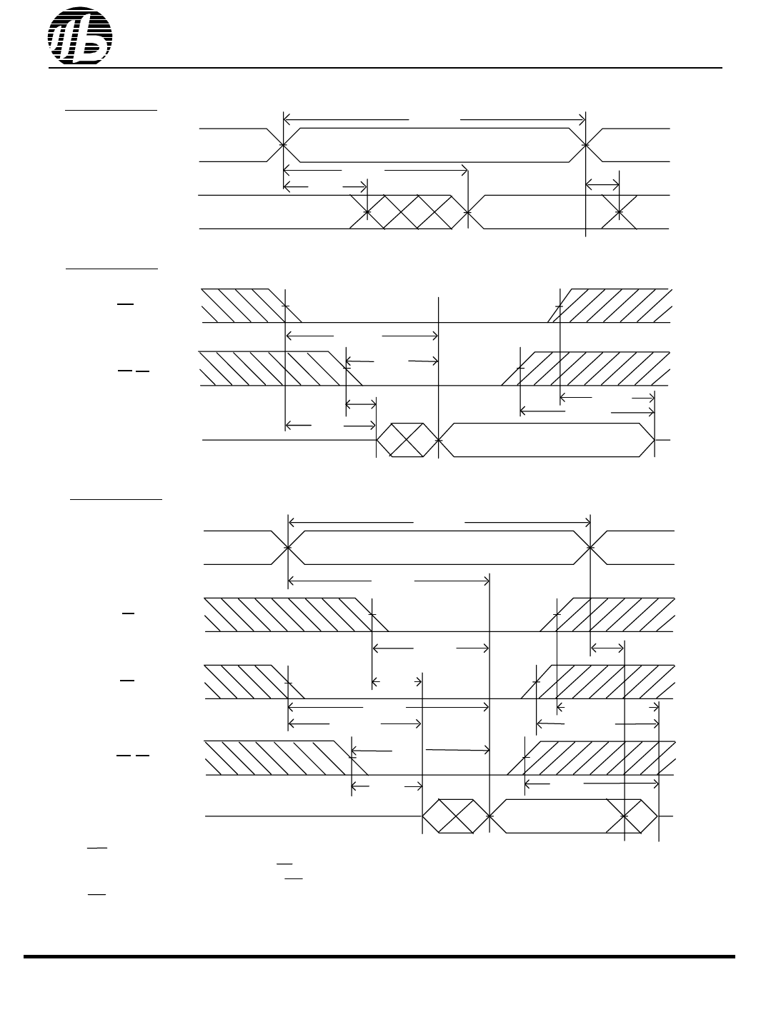
SWITCHING WAVEFORMS (READ CYCLE)
READ CYCLE1 (1,2,4)
t RC
ADDRESS
t OH
t AA
D OUT
READ CYCLE2 (1,3,4)
BS616LV1013
t OH
CE
LB,UB
D OUT
t ACS
t BA
(5)
t CLZ
t BE
t (5)
CHZ
t BDO
READ CYCLE3 (1,4)
ADDRESS
t RC
t AA
OE
t OE
CE
LB,UB
t OLZ
t(5) ACS
t CLZ
t BA
t BE
D OUT
NOTES:
1. WE is high for read Cycle.
2. Device is continuously selected when CE = VIL.
3. Address valid prior to or coincident with CE transition low.
4. OE = VIL .
5. Transition is measured ± 500mV from steady state with CL = 5pF as shown in Figure 1B.
The parameter is guaranteed but not 100% tested.
t OH
t OHZ (5)
t (1,5)
CHZ
t BDO
R0201-BS616LV1013
5
Revision 1.1
Jan. 2004
Share Link: 