74LVT2952 查看數據表(PDF) - Philips Electronics
零件编号
产品描述 (功能)
比赛名单
74LVT2952 Datasheet PDF : 12 Pages
| |||
Philips Semiconductors
3.3V Octal registered transceiver (3-State)
Product specification
74LVT2952
FEATURES
• 8-bit registered transceiver
• Independent registers for A and B buses
• Output capability: +64mA/-32mA
• TTL input and output switching levels
• Input and output interface capability to systems at 5V supply
• Bus-hold data inputs eliminate the need for external pull-up
resistors to hold unused inputs
• Live insertion/extraction permitted
• No bus current loading when output is tied to 5V bus
• Power-up reset
• Power-up 3-State
• Latch-up protection exceeds 500mA per JEDEC Std 17
• ESD protection exceeds 2000V per MIL STD 883 Method 3015
and 200V per Machine Model
DESCRIPTION
The LVT2952 is a high-performance BiCMOS product designed for
VCC operation at 3.3V.
This device combines low static and dynamic power dissipation with
high speed and high output drive.
The 74LVT2952 device is an 8-bit registered transceiver. Two 8-bit
back-to-back registers store data flowing in both directions between
two bidirectional buses.
Data applied to the inputs is entered and stored on the rising edge of
the Clock (CPXX) provided that the Clock Enable (CEXX) is Low.
The data is then present at the 3-State output buffers, but is only
accessible when the Output Enable (OEXX) is Low. Data flow from
A inputs to B outputs is the same as for B inputs to A outputs.
QUICK REFERENCE DATA
SYMBOL
PARAMETER
tPLH
tPHL
CIN
CI/O
ICCZ
Propagation delay
CPBA to An or
CPAB to Bn
Input capacitance
I/O pin capacitance
Total supply current
CONDITIONS
Tamb = 25°C; GND = 0V
CL = 50pF; VCC = 3.3V
VI = 0V or 3.0V
Outputs disabled; VI/O = 0V or 3.0V
Outputs disabled; VCC = 3.6V
TYPICAL
3.1
3.8
4
8
0.13
UNIT
ns
pF
pF
mA
ORDERING INFORMATION
PACKAGES
24-Pin Plastic SOL
24-Pin Plastic SSOP Type II
24-Pin Plastic TSSOP Type I
TEMPERATURE RANGE
–40°C to +85°C
–40°C to +85°C
–40°C to +85°C
OUTSIDE NORTH AMERICA
74LVT2952 D
74LVT2952 DB
74LVT2952 PW
NORTH AMERICA
74LVT2952 D
74LVT2952 DB
7LVT2952PW DH
DWG NUMBER
SOT137-1
SOT340-1
SOT355-1
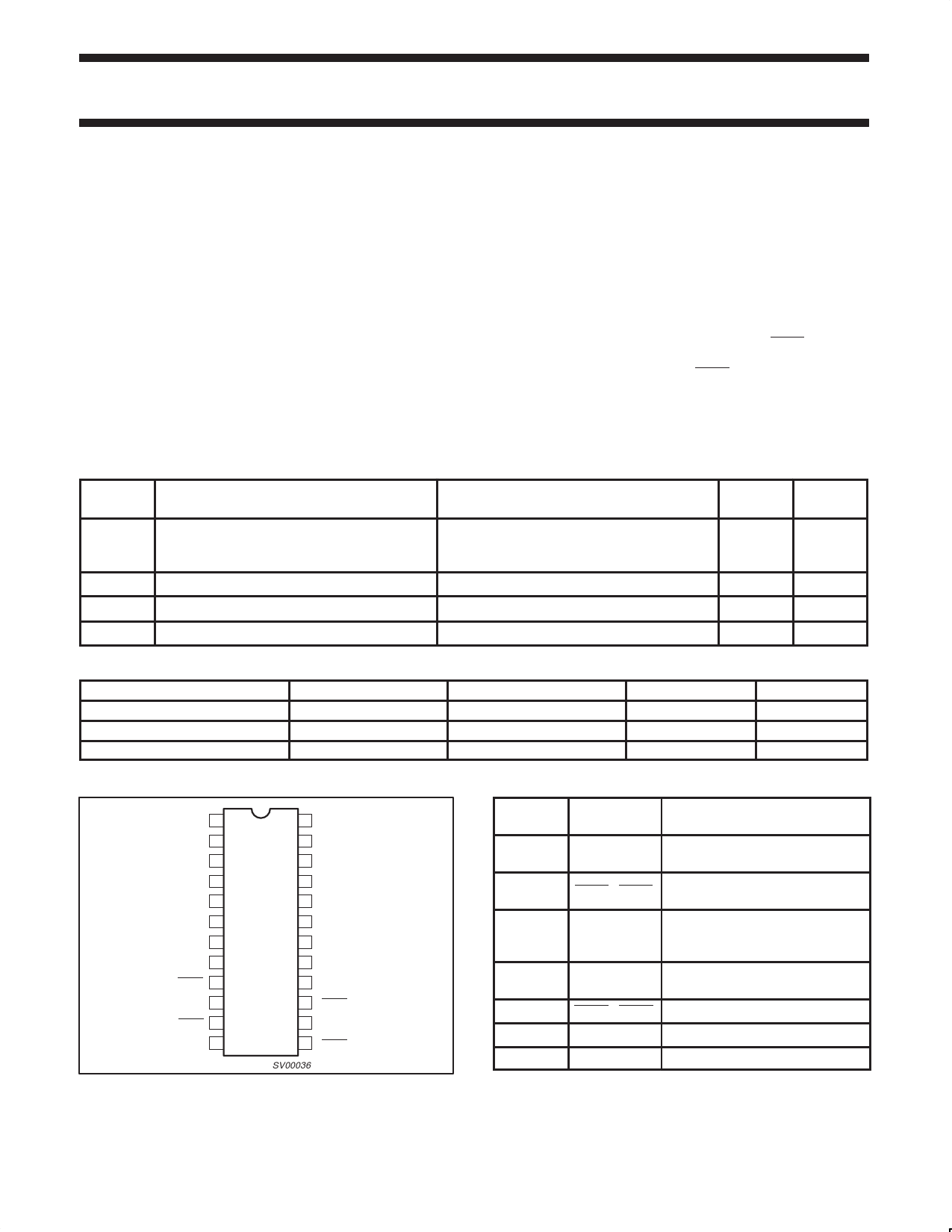
PIN CONFIGURATION
B7 1
B6 2
B5 3
B4 4
B3 5
B2 6
B1 7
B0 8
OEAB 9
CPAB 10
CEAB 11
GND 12
24 VCC
23 A7
22 A6
21 A5
20 A4
19 A3
18 A2
17 A1
16 A0
15 OEBA
14 CPBA
13 CEBA
SV00036
PIN DESCRIPTION
PIN
NUMBER
SYMBOL
10, 14 CPAB / CPBA
11, 13 CEAB / CEBA
16, 17, 18,
19, 20, 21,
22, 23
A0 – A7
8, 7, 6, 5,
4, 3, 2, 1
B0 – B7
9, 15 OEAB / OEBA
12
GND
24
VCC
NAME AND FUNCTION
Clock input A to B /
Clock input B to A
Clock enable input A to B /
Clock enable input B to A
Data inputs/outputs (A side)
Data outputs/outputs (B side)
Output enable inputs
Ground (0V)
Positive supply voltage
1998 Feb 19
2
853-1765 18987
Share Link: 